CSP Programming Strategies for the C-Suite
Originally published in Vol. 18, No. 2 of Global SMT & Packaging Magazine
 Good things come in small packages, but small packages can be tricky and costly to handle. The trend for higher density devices and smaller package sizes creates a unique set of challenges for the programming centers and manufacturers programming those devices. A light puff of air sends small parts flying, and misalignment of less than .2mm creates placement issues. This article shares best practices decision-makers should consider when purchasing or upgrading production equipment to program small IC devices to maximize speed, quality, and cost savings.
The rise in demand for small device packages
Mobile phones, PDAs, and other mobile products continue to take on new roles such as digital cameras, video cameras, and TV receivers. These functions require an increased number and greater variety of semiconductors in order to operate, while consumers want their finished products in ever-smaller form factors. Thus, as mobile phone sales have soared, demand for the chip-scale package (CSP) has increased faster than any other IC package type over the past decade or so. The demand for smaller packages with higher densities affects other segments including automotive, industrial, medical device, and Internet-of-Things. As the need for complex electrical circuits increases, programmed devices are developed in smaller and smaller packages to free up much-needed space in circuit design. As a result, programming centers and manufacturers are moving towards purchasing or retrofitting existing pick and place machines that are capable of programming such devices with little or no device failures.
Manufacturer challenges handling small devices
 Pick and place errors account for the majority of quality issues when programming small devices. Pick and place inaccuracy occurs when the machine is not taught precisely or is inaccurately placing parts due to unaccounted longer x-y axis settling times before a place. Teaching the z-height for a machine manually is nearly impossible for small devices, and for larger devices, operator skill and experience are required. Programming centers and manufacturers incur added costs for labor, machine idle time, lost devices, damaged devices, escapes, and poor yield.
Process control improvements
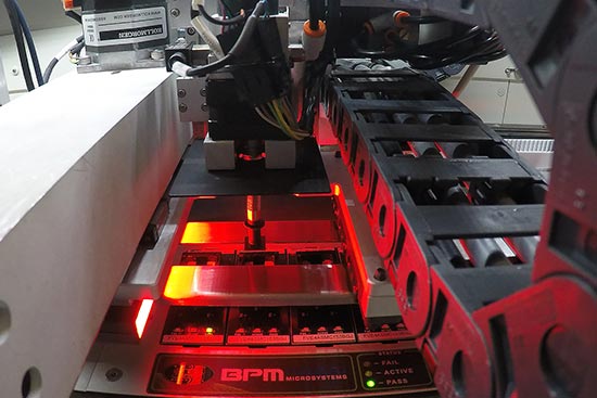
Automated IC device programmers lift and move devices using a vacuum nozzle attached to a robotic machine to perform repetitive operations. The negative pressure lifts the object and holds it against the nozzle while moving it to the desired location and then setting it into place. However, very small objects, such as a small computer or digital chips, including Wafer Level Chip Scale Packaging (WLCSP), small-outline transistors (SOT), and dual-flat no-leads (DFN), may be lifted by the nozzle prior to contact by the nozzle with the object. The vacuum may cause the object to “jump” up to the nozzle.
Operators using process control software teach the robotic machine the height of the object before it begins repetitive production operations. When setting up a job, operators use the process control software to teach the robotic machine the location (x, y, and z) of the input media, output media, peripherals, and programming site and socket. To teach z-height, the operator depresses the nozzle on the handler until it just touches the device. With IC device packages getting smaller, reaching .305mm thick and sizes of 1.7mm x 1.4mm, manually teaching the z-height of the device into the socket is nearly impossible. An operator cannot clearly see deep into the socket to see when the nozzle touches the device. With a flashlight and the assistance of a co-worker, multiple attempts and adjustments occur to determine the z-height.
During a teach cycle, the jump by the device causes the height to be measured incorrectly by the robotic machine that moves the nozzle. Subsequently, during repetitive operations, this incorrect height causes the machine to attempt to pick up the object before making contact. This leads to pick and place errors, dropped parts, cracked parts, and continuity errors. If alignment is off by even .2mm, the teach process must be repeated to avoid cracking or otherwise damaging the device.
Customers report manual teaching small devices takes up to 30 minutes per station. For programming centers with five changeovers per day, this costs 2.5 hours of machine idle time plus the costs of labor and lost or damaged devices. Programming centers and manufacturers should consider process control software and equipment with automated teaching capabilities for small parts. For example, BPM Microsystems WhisperTeach™ automates the task for the operator. It completes the task in 4.37 minutes with a standard deviation of 0.5mils, resulting in a savings of up to 25.63 minutes per station or 2.14 hours per day with five changeovers per day.
Accurately taught jobs improve yield by eliminating pick or place errors. Customers have reported yields as poor as 80% on very small parts using manual teach depending on operator skill. Process control software with automated z-height teaching produces a job yield of 99.99% by eliminating any teach-related issues.
Production control efficiencies
After completing the job setup and production begins, the accuracy of placement is critical to avoid damaging the device. Manufacturers need to ensure their systems self-calibrate z-height during production to eliminate the need for manual adjustments to compensate for variations in atmospheric pressure, nozzle size, flow rates, filter conditions, and more. This self-calibration by the machine ensures accurate handling throughout the job. In addition to intelligent process control software and pneumatics systems, look for systems equipped with a high-quality vision system to ensure the proper alignment of small parts before placement at each station. When integrated with the production software, vision systems allow the machine to align the device while in motion at high speeds.
For small parts, placement accuracy can be a challenge for systems that are unable to settle their x-y motion fast enough. Look for systems with designs allowing them to operate at maximum throughput without having to slow down the system to handle small parts. Customers achieve faster throughput and better reliability with a well-designed motion system.
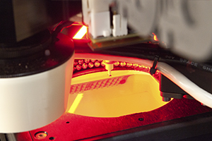
3D inspection to increase the quality

■ Precise Laser Micromark Measuring .1mm x .1mm.
Manufacturers looking to reduce scrap monitor each stage of the manufacturing process and take corrective action early. Device programming systems equipped with 3D inspection systems identify damaged parts early in the process. This allows manufacturers to take quick corrective action, resulting in higher quality, minimized reflow and lower overall costs.
3D inspection systems provide full device package validation after programming. High-performance systems support the verification of a variety of device packages including BGA, CSP, QFP, TSOP, SOIC, and J-Lead devices. When looking for an inspection system, features should include measurements for coplanarity, bent lead, pitch, width, diameter, standoff and XY errors.
Inspecting the coplanarity on leaded devices, such as the SOT-23 that measures 2.2mm x 2.7mm, ensures you do not exceed the manufacturer tolerance, which can create long-term reliability concerns of the device. The stress from bent leads may cause cracks in the package, reducing resistance against moisture and consequently present failure in the field due to internal corrosion. 3D inspection systems also identify devices with defective or missing balls on a BGA. By recognizing and removing damaged devices before final placement, manufacturers can prevent quality issues that would otherwise escape. This, in turn, improves production yield and process stability.
Laser marking for traceability
Manufacturers must thoroughly implement traceability control to maintain and confirm quality. Marking a device with a serial number, for example, enables traceability to the programming system, the site, and even the socket that programmed the device.
Smaller, thinner devices require fine control of the laser power to avoid damaging the device. Additionally, smaller devices require higher resolution marking capabilities. When purchasing a laser for your device programming system, look for a hybrid laser system that combines fiber and Nd:YAG laser technologies for precision marketing quality. Micromarking information in a limited space requires ultra-fine marketing capabilities, which is impossible with conventional laser marketing systems. Hybrid laser marking utilizes fine laser setting control, resulting in shallower marks, vivid coloration, and a lower thermal impact.
By recognizing and removing damaged devices before final placement, manufacturers can prevent quality issues that would otherwise escape. This, in turn, improves production yield and process stability.
A laser with a power monitor control provides high precision calibration of the laser mark, allowing accurate measure and control of laser energy output. The ability to monitor and control the laser power avoids damage to the device and reduces scrap. In electronics manufacturing, device damage affects quality, reliability, and profitability. A hybrid laser is an optimal solution for small device marking applications where it is necessary to eliminate the effect of heat transfer and control the maximum penetration depth while also providing high-contrast micromarking.
Conclusion
Modern electronic products favor higher density devices in smaller package sizes. Manufacturers and programming centers are purchasing or upgrading existing IC device programming systems to support the demands of programming small devices. A unique set of challenges exist to pick the small device out of tape, place it in the socket, program the device, laser mark the device, inspect the device through 3D inspection, and then place it out to tape. All of this needs to happen quickly, efficiently, and with high quality. Decision-makers need to consider many requirements when selecting an IC device programming system capable of handling small parts. Ensure the process control software and pneumatic system are qualified for small part handling and automatically teach z-height. Look for a self-calibrating machine with a high-performance vision system capable of aligning devices at high speed, on-the-fly, during production to maximize DPH. Systems with well-designed motion systems achieve faster throughput and higher reliability. Invest in a hybrid laser with power monitoring controls and micromarking capabilities to ensure device traceability. Finally, select a 3D inspection system that performs full device validation after programming, including checks for bent leads and defective balls, for quality and lower overall costs. Following these strategies will ensure your IC device programming system handles small devices with the speed, quality, and overall cost savings required for modern electronics manufacturing.
Link to original article
Originally published in the February 2018 edition of Global SMT & Packaging
SRIVATSAN MANI
Srivatsan Mani was the Director of Engineering who works with electronics manufacturers and programming centers to innovate solutions that modernize and improve their businesses. With more than 16 years of experience working with device programming systems, process control software, and device programming technology at BPM Microsystems, Inc., Srivatsan knows how to leverage technology to speed up the process while producing higher quality products at lower overall costs. Srivatsan led the development of the award-winning VectorEngine™ site programming technology, patented WhisperTeach™ automated z-height teaching solution, and BPWin™ process control software. Srivatsan holds a degree in electronics and communication engineering and masters in computer systems engineering.