
Types of Devices for Device Programming
BPM programmers offer high-performance device programming, advanced serialization, and quality control, meeting the highest programming and cybersecurity standards for automotive, aerospace, medical, industrial, and mobile device applications. Here is a list of some of the types of devices BPM programs.
Summaries are from Wikipedia
 Antifuse
Antifuses are widely used to permanently program integrated circuits (ICs).
Certain programmable logic devices (PLDs), such as structured ASICs, use fuse technology to configure logic circuits and create a customized design from a standard IC design. Antifuse PLDs are one-time programmable in contrast to other PLDs that are SRAM-based and which may be reprogrammed to fix logic bugs or add new functions. Antifuse PLDs have advantages over SRAM-based PLDs in that like ASICs, they do not need to be configured each time power is applied. They may be less susceptible to alpha particles which can cause circuits to malfunction. Also, circuits built via the antifuse’s permanent conductive paths may be faster than similar circuits implemented in PLDs using SRAM technology. QuickLogic Corporation refers to their antifuses as “ViaLinks” because blown fuses create a connection between two crossing layers of wiring on the chip in the same way that a via on a printed circuit board creates a connection between copper layers.
Antifuses may be used in programmable read-only memory (PROM). Each bit contains both a fuse and an antifuse and is programmed by triggering one of the two. This programming, performed after manufacturing, is permanent and irreversible.
 Chip-scale package
A chip-scale package (CSP) is a type of integrated circuit package.[1]
Originally, CSP was the acronym for chip-size packaging. Since only a few packages are chip size, the meaning of the acronym was adapted to chip-scale packaging. According to IPC‘s standard J-STD-012, Implementation of Flip Chip and Chip Scale Technology, in order to qualify as chip scale, the package must have an area no greater than 1.2 times that of the die and it must be a single-die, direct surface mountable package. Another criterion that is often applied to qualify these packages as CSPs is their ball pitch should be no more than 1 mm.
All of BPM’s Automated Systems can handle CSPs as small as 0402 (.4mm x .2mm).
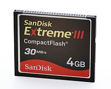 CompactFlash
CompactFlash (CF) is a flash memory mass storage device used mainly in portable electronic devices. The format was specified and the devices were first manufactured by SanDisk in 1994.[3]
CompactFlash became one of the most successful of the early memory card formats, surpassing Miniature Card and SmartMedia. Subsequent formats, such as MMC/SD, various Memory Stick formats, and xD-Picture Card offered stiff competition. Most of these cards are smaller than CompactFlash while offering comparable capacity and speed. Proprietary memory card formats for use in professional audio and video, such as P2 and SxS, are faster, but physically larger and more costly.
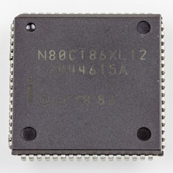
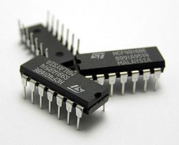 Dual in-line package
In microelectronics, a dual in-line package (DIP or DIL[1]), or dual in-line pin package (DIPP)[2] is an electronic component package with a rectangular housing and two parallel rows of electrical connecting pins. The package may be through-hole mounted to a printed circuit board (PCB) or inserted in a socket. The dual-inline format was invented by Don Forbes, Rex Rice and Bryant Rogers at Fairchild R&D in 1964,[3] when the restricted number of leads available on circular transistor-style packages became a limitation in the use of integrated circuits.[4] Increasingly complex circuits required more signal and power supply leads (as observed in Rent’s rule); eventually microprocessors and similar complex devices required more leads than could be put on a DIP package, leading to development of higher-density chip carriers. Furthermore, square and rectangular packages made it easier to route printed-circuit traces beneath the packages.
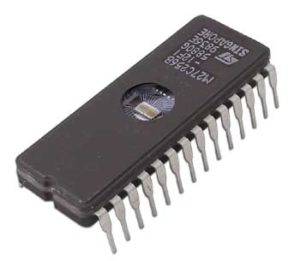 EPROM
EPROM
An EPROM (rarely EROM), or erasable programmable read-only memory, is a type of programmable read-only memory (PROM) chip that retains its data when its power supply is switched off. Computer memory that can retrieve stored data after a power supply has been turned off and back on is called non-volatile. It is an array of floating-gate transistors individually programmed by an electronic device that supplies higher voltages than those normally used in digital circuits. Once programmed, an EPROM can be erased by exposing it to a strong ultraviolet light source (such as from a mercury-vapor lamp). EPROMs are easily recognizable by the transparent fused quartz window in the top of the package, through which the silicon chip is visible, and which permits exposure to ultraviolet light during erasing.
MCU
A microcontroller (MCU for microcontroller unit) is a small computer on a single metal-oxide-semiconductor (MOS) integrated circuit (IC) chip. In modern terminology, it is similar to but less sophisticated than, a system on a chip (SoC); a SoC may include a microcontroller as one of its components. A microcontroller contains one or more CPUs (processor cores) along with memory and programmable input/output peripherals. Program memory in the form of ferroelectric RAM, NOR flash, or OTP ROM is also often included on-chip, as well as a small amount of RAM. Microcontrollers are designed for embedded applications, in contrast to the microprocessors used in personal computers or other general-purpose applications consisting of various discrete chips.
Microcontrollers are used in automatically controlled products and devices, such as automobile engine control systems, implantable medical devices, remote controls, office machines, appliances, power tools, toys and other embedded systems. By reducing the size and cost compared to a design that uses a separate microprocessor, memory, and input/output devices, microcontrollers make it economical to digitally control even more devices and processes. Mixed signal microcontrollers are common, integrating analog components needed to control non-digital electronic systems. In the context of the internet of things, microcontrollers are an economical and popular means of data collection, sensing and actuating the physical world as edge devices.
BPM is #1 Worldwide in MCU support
 Quad Flat Package
A QFP or Quad Flat Package is a surface-mounted integrated circuit package with “gull wing” leads extending from each of the four sides.[1] Socketing such packages is rare and through-hole mounting is not possible. Versions ranging from 32 to 304 pins with a pitch ranging from 0.4 to 1.0 mm are common. Other special variants include low-profile QFP (LQFP) and thin QFP (TQFP).[2]
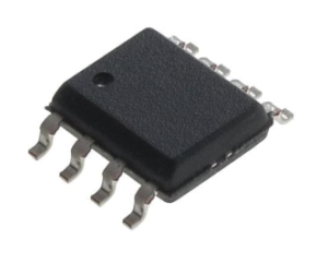 SOT
SOT
A small outline transistor (SOT) is a family of small footprint, discrete surface mount transistor commonly used in consumer electronics. The most common SOT are SOT23 variations,[1] also manufacturers offer the nearly identical thin small outline transistor (TSOT) package, where lower height is important.[2][3] [4][5]
 TSOP
TSOP
Thin Small Outline Package (TSOP) is a type of surface mount IC package. They are very low-profile (about 1mm) and have tight lead spacing (as low as 0.5mm).
They are frequently used for RAM or Flash memory ICs due to their high pin count and small volume. In some applications, they are being supplanted by ball grid array packages which can achieve even higher densities. The prime application for this technology is memory. SRAM, Flash memory, FSRAM and E2PROM manufacturers find this package well suited to their end-use products. It answers the needs required by telecom, cellular, memory modules, PC cards (PCMCIA cards), wireless, netbooks and countless other product applications.
TSOP is the smallest leaded form factor for flash memory.[1] The TSOP package was developed to fit the reduced package height available in a PCMCIA PC Card.[2] TSOPs are rectangular in shape and come in two varieties: Type I and Type II. Type I ICs have the pins on the shorter side and Type II have the pins on the longer side.
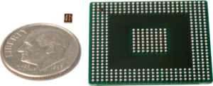
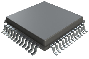
BGA
A ball grid array (BGA) is a type of surface-mount packaging (a chip carrier) used for integrated circuits. BGA packages are used to permanently mount devices such as microprocessors. A BGA can provide more interconnection pins than can be put on a dual in-line or flat package. The whole bottom surface of the device can be used, instead of just the perimeter. The traces connecting the package’s leads to the wires or balls which connect the die to package are also on average shorter than with a perimeter-only type, leading to better performance at high speeds.
Soldering of BGA devices requires precise control and is usually done by automated processes.
 Chip Carrier
In electronics, a chip carrier is one of several kinds of surface-mount technology packages for integrated circuits (commonly called “chips”). Connections are made on all four edges of a square package; Compared to the internal cavity for mounting the integrated circuit, the package overall size is large.[1]
Chip carriers may have either J-shaped metal leads for connections by solder or by a socket, or may be lead-less with metal pads for connections. If the leads extend beyond the package, the preferred description is “flat pack“.[1] Chip carriers are smaller than dual in-line packages and since they use all four edges of the package it can have a larger pin count. Chip carriers may be made of ceramic or plastic. Some forms of chip carrier package are standardized in dimensions and registered with trade industry associations such as JEDEC. Other forms are proprietary to one or two manufacturers. Sometimes the term “chip carrier” is used to refer generically to any package for an integrated circuit.
Types of chip-carrier package are usually referred to by initialisms and include:
- BCC: Bump Chip Carrier[2]
- CLCC: Ceramic Leadless Chip Carrier[3]
- Leadless chip carrier (LCC): Leadless Chip Carrier, contacts are recessed vertically.[2]
- LCC: Leaded Chip Carrier[2]
- LCCC: Leaded Ceramic Chip Carrier[2]
- DLCC: Dual Lead-Less Chip Carrier (Ceramic)[2]
- PLCC: Plastic Leaded Chip Carrier[2][3]
- PoP: Package on package
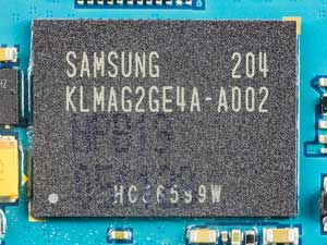 eMMC
eMMC
The eMMC (embedded MMC[7]) architecture puts the MMC components (flash memory plus controller) into a small ball grid array (BGA) IC package for use in circuit boards as an embedded non-volatile memory system. eMMC exists in 100, 153, 169 ball packages and is based on an 8-bit parallel interface.[8] This is noticeably different from other versions of MMC as this is not a user-removable card, but rather a permanent attachment to the circuit board. In the event of an issue stemming from either the memory or its controller, the PCB (printed circuit board) would need to be replaced or repaired.
Almost all mobile phones and tablets used this form of flash for main storage up to 2016, when UFS started to take control of the market. The latest version of the eMMC standard (JESD84-B51) by JEDEC is version 5.1A released January 2019, with speeds rivaling discrete SATA-based SSDs (400 MB/s).[9]
 Flatpack
Flatpack is a US military standardized printed-circuit-board surface-mount-component package. The military standard MIL-STD-1835C defines: Flat package (FP). A rectangular or square package with leads parallel to base plane attached on two opposing sides of the package periphery.
The standard further defines different types with varying parameters which includes package body material, terminal location, package outline, lead form and terminal count.
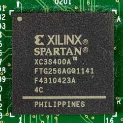 FPGA
FPGA
A field-programmable gate array (FPGA) is an integrated circuit designed to be configured by a customer or a designer after manufacturing – hence the term “field-programmable“. The FPGA configuration is generally specified using a hardware description language (HDL), similar to that used for an application-specific integrated circuit (ASIC). Circuit diagrams were previously used to specify the configuration, but this is increasingly rare due to the advent of electronic design automation tools.
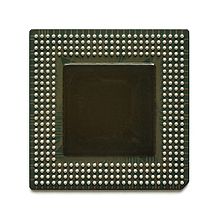
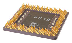 PGA
PGA
A pin grid array (PGA) is a type of integrated circuit packaging. In a PGA, the package is square or rectangular, and the pins are arranged in a regular array on the underside of the package. The pins are commonly spaced 2.54 mm (0.1″) apart,[1] and may or may not cover the entire underside of the package.
PGAs are often mounted on printed circuit boards using the through-hole method or inserted into a socket. PGAs allow for more pins per integrated circuit than older packages, such as dual in-line package (DIP).
Quad Flat No-leads package
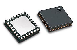 Flat no-leads packages such as quad-flat no-leads (QFN) and dual-flat no-leads (DFN) physically and electrically connect integrated circuits to printed circuit boards. Flat no-leads, also known as micro leadframe (MLF) and SON (small-outline no leads), is a surface-mount technology, one of several package technologies that connect ICs to the surfaces of PCBs without through-holes. Flat no-lead is a near chip scale plastic encapsulated package made with a planar copper lead frame substrate. Perimeter lands on the package bottom provide electrical connections to the PCB.[1] Flat no-lead packages include an exposed thermal pad to improve heat transfer out of the IC (into the PCB). Heat transfer can be further facilitated by metal vias in the thermal pad.[2] The QFN package is similar to the quad-flat package (QFP), and a ball grid array (BGA).
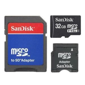 SD Cards
Secure Digital, officially abbreviated as SD, is a proprietary non-volatile memory card format developed by the SD Card Association (SDA) for use in portable devices.
The standard was introduced in August 1999 by joint efforts between SanDisk, Panasonic (Matsushita Electric) and Toshiba as an improvement over MultiMediaCards (MMC),[1] and has become the industry standard. The three companies formed SD-3C, LLC, a company that licenses and enforces intellectual property rights associated with SD memory cards and SD host and ancillary products.[2]
The companies also formed the SD Association (SDA), a non-profit organization, in January 2000 to promote and create SD Card standards.[3] SDA today has about 1,000 member companies. The SDA uses several trademarked logos owned and licensed by SD-3C to enforce compliance with its specifications and assure users of compatibility.[4]
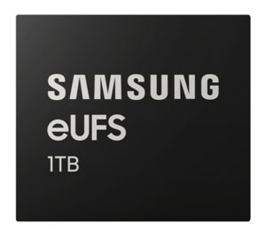 UFS
UFS
Universal Flash Storage, officially abbreviated as UFS, is a flash storage specification for digital cameras, mobile phones and consumer electronic devices.[1][2] It aims to bring higher data transfer speed and increased reliability to flash memory storage, while reducing market confusion and removing the need for different adapters for different types of card.[3]
The proposed flash memory specification is supported by leading firms in the consumer electronics industry such as Nokia, Sony Ericsson, Texas Instruments, STMicroelectronics, Samsung, Micron, SK Hynix.[4] UFS is positioned as a replacement for eMMCs and SD cards. The electrical interface for UFS uses the M-PHY,[5] developed by the MIPI Alliance, a high-speed serial interface targeting 2.9 Gbit/s per lane with up-scalability to 5.8 Gbit/s per lane.[6][7] UFS implements a full-duplex serial LVDS interface that scales better to higher bandwidths than the 8-lane parallel interface of eMMCs. Unlike eMMC, Universal Flash Storage is based on the SCSI architectural model and supports SCSI Tagged Command Queuing.[8][9]