+1 (713) 688-4600 | Sales Toll-Free: (855) SELL BPM | 24/7 Service: +1 (832) 617-5702 info@bpmmicro.com
Select Page
US Patent: Object detection system (WhisperTeach™)

US Patent: Object detection system (WhisperTeach™)

US Patent Approved 2/23/2021

An object detection system utilizes a teach cycle performed with an ingenious object detector that utilizes the pick-up nozzle. The height of the object is stored as the taught height to be used subsequently in repetitive operations by the machine. This teaching method is particularly useful for very small objects and is available on all BPM Automated Programming Systems. BPM calls this patented process WhisperTeach™.

WhisperTeach™ offers faster setup times and improved yields; it eliminates common Z-height errors such as miss picks, miss place, and socket continuity flaws. Very small devices such as WLCSP, SOT, DFN have very low mass. When teaching using a vacuum, the suction causes the part to jump up to the nozzle, increasing the possibility of an inaccurate Z teach elevation. Because it uses the pick-up nozzle to detect the object, the system knows precisely the exact coordinates without additional offset calculations.

Modern pick and place machines are highly repeatable. The quality of the repetitive pick/place process is dependent on the accuracy of the teach process. Human teaching can introduce repetitive inaccuracies. WhisperTeach is accurate to within 15microns; approximately 3x more accurate than humans can detect unaided.

WhisperTeach™ Page WhisperTeach Demo Press Release

US Patent: Automated teaching of pick and place workflow locations on an automated programming system

US Patent: Automated teaching of pick and place workflow locations on an automated programming system

Patent Number: US 2020/0148484 A1

Inventors: William H. White, Alain A. Mangiat, Josue E. Salazar Vanoye, Colin D. Harper

Abstract

The operator may first place a blank device in a first socket in a first site. The APS may self-teach the position and orientation of that first socket by removing and replacing the device in the socket one or more times, and by detecting the position of the device in the socket or by monitoring a change in position of the device as it is placed into the socket. The APS then picks the device from the first socket (or from the input tray) and moves it in succession through the rest of the sockets to establish position and orientation of each socket. After all sockets are taught, the APS loads all sockets with blank devices, and programming begins. Alternatively, the programming job begins as each site is taught and before the remaining sites are taught so that production output can begin “immediately.”
 

Description

BACKGROUND

The present disclosure relates to teaching the pick and place locations for an automated programming system job on an Automated Programming System, hereafter “APS.” Prior to this invention, operators were required to manually assist with teaching each device pick and place location using semi-automated methods. Operators were required to manually load and unload devices for each pick or place point and then assist the APS in determining the X, Y, Z, and Theta target location for each workflow pick or place point before the full productivity of the job could begin.

SUMMARY

Disclosed herein are automated methods to setup or teach the pick and place locations for an automated programming system job on an Automated Programming System, hereafter “APS.” This reduces the setup time, reduces the level of operator skill required and improves setup accuracy, improves job yield, and reduces the frequency of human intervention required. Once the system is configured with the blank devices that will be programmed, input/output peripherals, socket adapters, and the feature is invoked, the system will teach the job and begin processing (programming devices) without operator intervention.

With fully automated self-teaching, operator involvement in the job set-up process is greatly reduced. The initial job set-up of input/out locations and peripherals is familiar Blank devices in media (tape, tray, tube) are loaded and Input/Output peripheral locations are taught. From that point, the process becomes radically different and more productive.

Using multiple pick and place cycles and analyzing results with a mathematical model, the APS will automatically determine, retain and adjust as necessary the target locations for pick and place locations within the programming job workflow. The initial, imprecise locations may be predetermined at the factory before shipment, or subsequently established at the customer location. Alternatively, a camera will assist to identify and establish each target pick or place point using machine vision algorithms.

Each pick and place point has a predetermined location, unique to each APS. The operator may place a blank device in socket A in the master programming site (typically Site 1). The z-height of the first device will be used for all subsequent devices at the respective socket locations. The APS then picks the device from socket A and moves it in succession to sockets B through “n” to establish the X, Y, Z, and Theta locations for each socket. After the master site has been taught, the APS subsequently moves the device to all of the other sites and sockets installed on the machine. After all programming sites and sockets are taught, the device is placed in socket A of the master site, the APS loads all sockets with blank devices, and programming begins.

Alternatively, the programming job begins as each site is taught and before the remaining sites are taught so that production output can begin “immediately.” Alternatively, all parts are placed into sites automatically using computed locations and/or machine vision or sensors. Alternatively, additional teach locations such as input peripherals, output peripherals, and marking peripherals are taught automatically. Alternatively, another method is used to teach the Z height.

The operator can walk away from the APS as soon as the auto-teach process begins. The machine then proceeds to teach and start running the job autonomously. In prior implementations, the operator had to continue to give the machine attention and was unable to walk away from the APS until the job started running.

In one embodiment, the operator only has to manually place at most one device into a socket. In prior implementations, the operator was required to place multiple devices into sockets.

In one embodiment, each blank device that is used for teaching is used to teach at most one socket. In prior implementations, a single device was moved from socket to socket to teach multiple sockets, which could cause some mechanical degradation of the device.

This automated system offers greater accuracy and repeatability than human operators. By automatically identifying, predicting, and teaching each pick and place location within the APS workflow, job setup time can be greatly reduced, leading to higher system productivity per job and per year. Further, teaching accuracy and repeatability improves system yield and quality. By automating the teaching process, the requirement for highly skilled operators is reduced, potentially lower the labor burden for the programming process.

US Patent: Electronic apparatus and bit error rate tolerance method for programming non-volatile memory devices

US Patent: Electronic apparatus and bit error rate tolerance method for programming non-volatile memory devices

US Patent: Electronic apparatus and bit error rate tolerance method for programming non-volatile memory devices

US Patent 2009/0287969

Inventors: Brandon L. White, Danny Tjandra

Abstract

The present invention provides an apparatus and method for using a bit error rate tolerance (BERT) technique for high-speed programming of non-volatile electronic memory devices. The device programmer is comprised of an embedded computer system and specialized electronic circuitry to interface to the device to be programmed. According to one aspect of the invention, the device programmer contains digital registers to accumulate the number of incorrect data bits encountered during the verification of the device programming operation. A field-programmable input to the device programmer specifies the BERT to be allowed at precise intervals within the device. Devices that are found to exceed the specified BERT shall be rejected.

Description

This application claims priority from U.S. Provisional Patent Application No. 61/052,889, filed May 13, 2008, entitled “ELECTRONIC APPARATUS AND BIT ERROR RATE TOLERANCE METHOD FOR PROGRAMMING NON-VOLATILE MEMORY DEVICES.” This application is hereby incorporated by reference in its entirety for all purposes.

BACKGROUND OF THE INVENTION

1. Field of Invention

The present invention relates to the field of automated transfer of electronic data into non-volatile digital memory devices. In particular, the present invention relates to electronic systems and methods for the detection of erroneous data occurring in such devices during data transfer.

2. Description of the Related Art
In the electronics manufacturing industry, it is often desirable to transfer data into a non-volatile semiconductor device, such as flash memory, using special-purpose programming machines known as device programmers. Employing device programmers to handle this task is often necessary to achieve an initial state in the device such that it may then be assembled into a larger electronic system, known as an embedded system. This pre-programming of an initial state allows the manufactured system to achieve basic functionality for further programming of the device by other means, usually as a function of the manufactured embedded system itself. This practice may also extend to other areas related to electronics manufacturing that include, but are not limited to, research and development, and failure analysis.

It is often practical to utilize the device programmer to pre-program all intended data into the device during manufacture as a cost reduction technique. Embedded systems may have particular design attributes such as low power consumption combined with reduced performance processing units that achieve less than maximal data transfer rates of the memory device. Device programmers can often achieve much more rapid transfer times which can increase the rate of system manufacture thereby lowering the per-unit manufacturing cost.

Certain types of modern, large capacity, non-volatile memory devices, such as NAND Flash, exhibit reliability errors in the data stored in the device. These errors manifest as output data that contains unpredictable differences from the original input data. The frequency of these errors increases with the repeated erasure and programming of the cells internal to the device. It is a burden of the system that interfaces to the flash device to detect and correct such errors, where possible.

To improve the accuracy of the data transferred out of a non-volatile memory device, e.g., a flash device, to a level acceptable by the application of the system, error correction code (ECC) algorithms are widely used. Such algorithms compute code values in relation to the data to be stored in the device. These code values are typically stored in the flash device itself along with the original data. Upon transfer of data output from the flash device, the code data is output as additional information. The system receiving the data from the flash device makes use of a decoding algorithm that utilizes the code to detect, and in most cases correct, incorrect binary data states in the received transfer.

A limitless number of practical implementations of ECC techniques exist. There are various encoding and decoding algorithms, and each can be varied in numerous ways to suit particular requirements as will be understood to those skilled in the art. The frequency and manner in which the code values are arranged in relation to the original data present yet another vast mixture of possibilities. Additionally, some systems are known to combine multiple ECC implementation techniques in a dynamic hybrid fashion (see, e.g., US Pat. App. Pub. No. 20040083333A1, which is hereby incorporated by reference).

ECC algorithms are designed in a manner such that the decoding operation indicates the number of individual bit errors present in the data transferred from the device, if any. Furthermore, an additional computation can then be performed in the event of such bit errors so as to correct these errors. Generally, ECC algorithms can correct some lesser number of errors than can be detected. For instance, a 4-bit ECC algorithm may be able to detect the presence of 5 or more invalid bits in a block of data, but is only capable of precisely identifying and thus correcting 4 of the erroneous bits. The integrity of the embedded system can be maintained so long as the bit error rate (BER) for any block of data transferred from the flash memory device does not exceed the correction limits of the ECC algorithm used to encode that data block.

ECC algorithms require complex computations and as such incur latencies when the system accesses the data in the device. Generally, the stronger the ECC algorithm in terms of the number of bit correction ability, the more computational overhead is required. ECC algorithms may be implemented as software instructions for a processing unit, or may be implemented in whole or in part on dedicated hardware logic circuitry to increase the performance of the computations.

When pre-programming a NAND flash device by way of a device programming machine, data corruption failures must be detected. If these failures exceed the limits of the target embedded system’s ECC algorithm correction capability, then the device must be rejected and excluded from further assembly into the target system circuit.

In the prior art, device programmers leveraged the assumption that NAND flash devices would not yield bit errors during manufacturing pre-programming due to the lack of disturbance issues in new devices. While this certainly remains true for Single Level Cell (SLC) NAND flash devices, Multiple Level Cell (MLC) devices can and will in fact experience program disturbance issues on the first and subsequent program operations that will lead to incorrect bit states upon transfer of the data from the device.

Applying conventional device programmer methods to MLC NAND flash devices results in unsuccessful yield, as nearly all devices would be rejected by the machine upon detection of the erroneous data bits in the output.

Implementing the ECC algorithm used by the embedded system in the device programmer is an obvious but inadequate solution. The computational overhead for these algorithms is not suitable for the rates desired for electronics manufacturing. Furthermore, the exact details of any particular embedded system’s ECC methods might be difficult or impossible to obtain. Advanced ECC methods are often proprietary, with multiple parties involved and the license for such use untenable. Lastly, the cost to develop such algorithms on a per-device, per-system basis is typically prohibitive.

Therefore, a need exists for a device programming machine with an improved method and apparatus for data verification within a bit error rate tolerance threshold. That is, what is desired is a method and apparatus for high-speed pre-programming of MLC NAND Flash or other non-volatile memory devices within the capabilities of any arbitrary ECC algorithm without employing such algorithms directly.

BRIEF SUMMARY

Briefly, the present invention provides an apparatus and method for using a bit error rate tolerance (BERT) technique for high-speed programming of non-volatile electronic memory devices. The device programmer, in certain aspects, includes an embedded computer system and specialized electronic circuitry to interface to the device to be programmed.

According to one embodiment, a method for using a bit error rate tolerance technique during high-speed programming of non-volatile memory devices is disclosed. The method comprises receiving a tolerance value representing a maximum number of bit errors that a memory region in a non-volatile memory device can tolerate. Next, the method analyzes a memory region of the non-volatile memory device to find the number of bit errors contained in the memory region of the device without running an error correcting code algorithm. The method then compares the number of bit errors found in the analyzed memory region of the non-volatile memory device to the tolerance value. Non-volatile memory devices in which the number of bit errors found in the analyzed memory region of the non-volatile memory device is greater than the tolerance value are then rejected.

According to another embodiment, a device programmer apparatus for programming a non-volatile memory device is disclosed. The apparatus comprises a means for storing data to be transferred into memory of a non-volatile memory device, a means for transferring data into memory of the non-volatile memory device, a means for analyzing a memory region of the non-volatile memory device that stores the transferred data to find the number of bit errors contained in the memory region without running an error correcting code algorithm, a means for comparing the number of bit errors found in the analyzed memory region of the non-volatile memory device to a tolerance value representing a maximum number of bit errors that a memory region in the memory device can tolerate, and a means for rejecting the non-volatile memory device if the number of bit errors found in the analyzed memory region of the non-volatile memory device is greater than the tolerance value.

According to another embodiment, a computer readable medium with computer-executable code is disclosed. The computer-readable medium comprises code for receiving a tolerance value representing a maximum number of bit errors that a memory region in a non-volatile memory device can tolerate, code for analyzing a memory region of the non-volatile memory device to find the number of bit errors contained in the memory region of the device without running an error correcting code algorithm, code for comparing the number of bit errors found in the analyzed memory region of the non-volatile memory device to the tolerance value, and code for rejecting the non-volatile memory device if the number of bit errors found in the analyzed memory region of the non-volatile memory device is greater than the tolerance value.

According to another embodiment of the invention, a device programmer contains digital registers to accumulate the number of incorrect data bits encountered during the verification of the device programming operation. A field-programmable input to the device programmer specifies a bit error rate tolerance (BERT) to be allowed at precise intervals within the device. Devices that are found to exceed the specified BERT can be rejected and visually indicated as such by the machine.

According to another embodiment of the present invention, a BERT input is set according to the ECC capabilities of the target system into which the device will be assembled. A device programmer will only indicate successful programming status for devices that contain a number of bit errors equal to or less than the correction capabilities of the target system’s ECC algorithm. Devices failing to meet this specification can be rejected and visually indicated as such by the machine to prevent further assembly of the device into the target system, thereby avoiding the assembly of a non-functional target system.

In another embodiment, an apparatus includes the circuitry and implements simultaneous programming of multiple quantities of devices. Each device’s error statistics are computed and retained discretely by the device programmer circuitry in real-time, as is necessary to manage the random distribution of possible error bits on individual devices.

According to still another aspect of the present invention, multiple BERT inputs may be specified by the operator of the device programmer, as desired, to accommodate varying tolerances for different memory regions of the memory device.

Further aspects and advantages of the present invention shall become apparent upon reading and understanding the following detailed descriptions of example embodiments and studying the various figures of the drawings.

US Patent: In-line program system for assembly printed circuit board

US Patent: In-line program system for assembly printed circuit board

Abstract

An in-line programming (ILP) system and method for programming and testing programmable integrated circuit devices (PICs) and performing the assembly of printed circuit board assemblies (PCBAs). Printed circuit boards enter and leave the ILP system on a conveyor system. PICs are loaded into the ILP system, and the ILP system automatically programs and tests the PICs and places them onto the PCBs as the PCBs arrive on the conveyor. The programming and testing operations are performed by the same piece of equipment that performs the PCBA assembly operation.

Inventor: William H. White
Current Assignee: BPM Microsystems Inc
Worldwide applications: 2000 EP WO AU US JP 2001 US 2004 US 2006 US

Description

This application is a division of U.S. patent application Ser. No. 09/776,095, filed Feb. 1, 2001, now U.S. Pat. No. 6,687,986, which is a continuation of U.S. patent application Ser. No. 09/493,953, filed Jan. 28, 2000, now U.S. Pat. No. 6,230,067, entitled “In-Line Programming System and Method,” which is related to U.S. Provisional Patent Application Ser. No. 60/117,873 filed Jan. 29, 1999, entitled “N-LINE PROGRAMMING DEVICE WITH SELF TEACHING CAPACITY,” and the disclosures of each are hereby incorporated by reference.

Background

The present invention generally relates to concurrent automated programming of programmable electronic devices, and more particularly to programming and testing multiple device types and patterns and performing circuit board assembly simultaneously in a single in-line programming device.

In the semiconductor industry, a considerable number of electronic devices such as programmable integrated circuit (PIC) devices are provided by vendors in a programmable form with blank memories or unspecified connections between arrays of logic. Users can then custom configure or program the electronic devices to perform their intended function by programming them, transferring or “burning in” a sequence of operating codes into the memory, or by specifying a particular arrangement of gating logic connections.

Numerous manufacturers have developed automated machinery for handling and programming such devices. Such machinery moves blank devices from a source medium (e.g., trays, tubes, tape) to one or more programming sites, carry out the programming operation on each device, and moves programmed devices from the programming sites to an output medium (e.g., trays, tubes, tape). Typical users of automated programming equipment are highly sensitive to system throughput, which is typically measured incorrectly programmed devices per hour, and yield, which is typically defined as the percentage of devices that are correctly programmed.

Before any printed circuit board assembly (PCBA) containing a programmable integrated circuit (PIC) can be used, the PIC must be configured or programmed, so that it may perform its intended function. During programming, a pattern is loaded into the unprogrammed PIC. These patterns may be changed from time to time as the requirements of the function of the PCBA change over time. Also, in some applications, the pattern may be individualized for each PCBA that is assembled.

For years, PICs have been programmed before being assembled onto a printed circuit board using a methodology called off-line programming (OLP). This, however, created some problems in that OLP of the PICs has to be performed prior to assembly. Specialized equipment must also be obtained to perform OLP. Further, OLP has to be scheduled, which may delay the manufacture of PCBAs and create scheduling problems and bottlenecks in the process. Moreover, once the PICs is programmed, they must be stored until the assembly process begins. This storage and related delay typically create an inventory of programmed PICs. Not only does this inventory cost money, but in the event that a pattern change is required immediately, the inventory of programmed PICs may have to be destroyed, which adds to the cost and creates an additional delay before the assembly of more PCBAs can commence.

To solve these problems, a technique called in-circuit programming (ICP) was developed. ICP allows for a PIC to be programmed after it is placed on a printed circuit board, i.e., after the PCBA is assembled. Thus, the need for an inventory of programmed devices was eliminated, and individualized PICs no longer needed to be matched with the corresponding PCBA because all the PICs are identical (unprogrammed) at assembly time.

However, new problems arose. For example, because it is not feasible to program all PICs in the circuit, the designers of the PCBA must choose only devices that are ICP compatible. ICP compatible PICs cost more than similar non-ICP compatible PICs in many cases, so the cost of the PCBA may be higher when using ICP. Additionally, the PCBA design may be more complex to accommodate ICP, so the time to market may be negatively impacted. Furthermore, specialized equipment is required, and software must be written, perform the programming operation, which also may impact time to market for the PCBA. Since the programming operation may take a number of minutes to perform, a production line may be slowed down waiting for programming to complete. To address this throughput problem, some users may set up several ICP programming stations to service a single PCBA assembly line. However, this solution requires additional equipment, floor space in the factory, and capital outlay. Additionally, if the application for the PCBA requires that the PICs be programmed with individualized patterns, it may be necessary to match the individual PICs with their corresponding individual PCBAs. This additional complication adds additional cost and complexity to the assembly operation. Finally, in the event that the PIC fails to program, the entire PCBA will have to be reworked to replace the PIC.

Accordingly, what is needed in the art is a system and methodology for programming PICs and assembling PCBAs without the drawbacks associated with the off-line programming and in-circuit programming techniques.

Summary

Briefly, the invention provides in-line programming techniques for programming and testing any combination of devices and patterns. The techniques of the present invention are useful for programming a variety of types of programmable integrated circuit devices (PICs), including, for example, flash memories, EEPROMs, microcontrollers, PLDs, PALs, FPGAs, and the like. According to the invention, in-line programming (ILP) system programs and tests PICs and performs the assembly of printed circuit board assemblies (PCBAs). Printed circuit boards enter and leave the ILP system on a conveyor system. PICs are loaded into the ILP system, and the ILP system automatically programs and tests the PICs and places them onto the PCBs as the PCBs arrive on the conveyor.

The present invention addresses all of the above problems (e.g., costs, complications, and delays) by performing the programming and testing operations with the same piece of equipment that performs the assembly operation. Using the techniques of the present invention, PICs are programmed on demand so the need for an inventory of programmed PICs is eliminated, and changes to the program pattern may be incorporated immediately without waste. Any PICs that fail to program are rejected by the ILP system so that bad PICs are never placed onto a PCBA. Because the PCBA does not have to be designed to accommodate an in-circuit programming technique, the PCBA designer is unconstrained in the choice of PICs. The ILP system generally programs PICs faster than PICs can be programmed using the in-circuit programming methodology. The ILP system is also able to program a number of devices simultaneously, allowing a PCBA assembly line to produce PCBAs at a faster pace than that at which a single PIC can be programmed. Thus, an assembly line incorporating an ILP system may be smaller and produce PCBAs faster, with higher quality and less expense than an assembly line incorporating an in-circuit programming system. Further, the use of an ILP system in an assembly line allows for PCBAs to be produced less expensively than in an assembly line incorporating programmed PICs from an off-line programming system.

According to an aspect of the present invention, a method of automatically assembling a printed circuit board assembly (PCBA) in an assembly apparatus is provided. The method typically comprises the steps of a) receiving, in the assembly apparatus, a programmable electronic device to be programmed, and b) automatically programming the electronic device in the assembly apparatus. The method also typically includes the steps of c) receiving a printed circuit board in the assembly apparatus, and d) assembling the PCBA in the assembly apparatus by automatically placing the programmed electronic device on the printed circuit board so as to form the PCBA.

According to another aspect of the present invention, an assembly apparatus capable of automatically assembling a printed circuit board assembly (PCBA) is provided. The apparatus typically comprises a means for receiving, in the assembly apparatus, a programmable electronic device to be programmed, and a means for automatically programming the electronic device in the assembly apparatus. The apparatus also typically includes a means for receiving a printed circuit board in the assembly apparatus, and a means for automatically placing the programmed electronic device on the printed circuit board so as to form the PCBA.

Reference to the remaining portions of the specification, including the drawings and claims, will realize other features and advantages of the present invention. Further features and advantages of the present invention, as well as the structure and operation of various embodiments of the present invention, are described in detail below with respect to the accompanying drawings. In the drawings, similar reference numbers indicate identical or functionally similar elements.

While the invention has been described by way of example and in terms of the specific embodiments, it is to be understood that the invention is not limited to the disclosed embodiments. On the contrary, it is intended to cover various modifications and similar arrangements as would be apparent to those skilled in the art. Therefore, the scope of the appended claims should be accorded the broadest interpretation so as to encompass all such modifications and similar arrangements.


Claims (9)

  1. A system for use within a surface mount production line having a conveyor for receiving a printed circuit board, and for moving the printed circuit board through the surface mount production line, the system comprising: a concurrent programming system containing first and second programming sites;

    a pick and place system for picking up first and second electronic devices from one or more tray shuttles, and for placing the first and second electronic devices within the first and second programming sites, respectively, the first and second electronic devices being programmable in a concurrent manner and independent of each other; and
    a central control unit for communicating with the conveyor, the concurrent programming system, and the pick and place system, the central control unit directing the conveyor to move the printed circuit board permitting the pick and place system to place the first and second electronic devices on the printed circuit board after the devices are programmed;

    wherein the conveyor system is controlled according to state variables associated with receiving a printed circuit board from an upstream device and providing an assembled printed circuit board assembly to a downstream device, and wherein the state variables include one or more of a first variable indicating that the upstream device is ready to deliver the printed circuit board, a second variable indicating that the downstream device is ready to receive the assembled printed circuit board assembly, a third variable indicating that the conveyor system is ready to receive the printed circuit board, and a fourth variable indicating that the conveyor system is ready to deliver the assembled printed circuit board assembly.

  2. The system of claim 1 wherein the concurrent programming system further comprises a controller for each of the first and second programming sites for independently programming each of the first and second programming sites.
  3. The system of claim 2 wherein the pick and place device further comprises a controller for servicing requests from the concurrent programming system and the conveyor.
  4. The system of claim 3 wherein the system making a request provides the location from which to pick up a device.
  5. The system of claim 1 further comprising tracks or rails enabling movement of the pick and place device within the system.
  6. The system of claim 1 further comprising one or more sensors for detecting when the conveyor delivers a printed circuit board to the system.
  7. The system of claim 1 further comprising four parallel asynchronous processes upon which operations of the system depend.
  8. The system of claim 1 wherein the pick and place device includes self-teaching capability for determining the precise locations at which to pick and place the first and second programmable devices.
  9. The system of claim 1 further comprising employing fiducial recognition techniques to determine the location at which the programmable device is to be placed.
US Patent: Method of programming a programmable electronic device by an in-line programming system

US Patent: Method of programming a programmable electronic device by an in-line programming system

US Patent No 6,687,986 B2

Inventor: William H. White

Abstract

An in-line programming (ILP) system and method for programming and testing programmable integrated circuit devices (PICs) and performing the assembly of printed circuit board assemblies (PCBAs). Printed circuit boards enter and leave the ILP system on a conveyor system. PICs are loaded into the ILP system, and the ILP system automatically programs and tests the PICs and places them onto the PCBs as the PCBs arrive on the conveyor. The programming and testing operations are performed by the same piece of equipment that performs the PCBA assembly operation.

Description

CROSS-REFERENCES TO RELATED APPLICATIONS
This application is a continuation of U.S. patent application Ser. No. 09/493,953, filed Jan. 28, 2000, now U.S. Pat. No. 6,230,067, entitled “In-Line Programming System and Method, ” which is related to U.S. Provisional Patent Application Serial No. 60/117,873, filed Jan. 29, 1999, entitled “IN-LINE PROGRAMMING DEVICE WITH SELF TEACHING CAPACITY,” the disclosure of each of which is incorporated by reference.

BACKGROUND OF THE INVENTION
The present invention generally relates to concurrent automated programming of programmable electronic devices, and more particularly to programming and testing multiple device types and patterns and performing circuit board assembly simultaneously in a single in-line programming device.

In the semiconductor industry, a considerable number of electronic devices such as programmable integrated circuit (PIC) devices are provided by vendors in programmable form with blank memories or unspecified connections between arrays of logic. Users can then custom configure or program the electronic devices to perform their intended function by programming them, transferring or “burning in” a sequence of operating codes into the memory, or by specifying a particular arrangement of gating logic connections.

Numerous manufacturers have developed automated machinery for handling and programming such devices. Such machinery moves blank devices from a source medium (e.g., trays, tubes, tape) to one or more programming sites, carry out the programming operation on each device, and moves programmed devices from the programming sites to an output medium (e.g., trays, tubes, tape). Typical users of automated programming equipment are highly sensitive to system throughput, which is typically measured incorrectly programmed devices per hour, and yield, which is typically defined as the percentage of devices that are correctly programmed.

Before any printed circuit board assembly (PCBA) containing a programmable integrated circuit (PIC) can be used, the PIC must be configured or programmed, so that it may perform its intended function. During programming, a pattern is loaded into the unprogrammed PIC. These patterns may be changed from time to time as the requirements of the function of the PCBA change over time. Also, in some applications, the pattern may be individualized for each PCBA that is assembled.

For years, PICs have been programmed before being assembled onto a printed circuit board using a methodology called off-line programming (OLP). This, however, created some problems in that OLP of the PICs has to be performed prior to assembly. Specialized equipment must also be obtained to perform OLP. Further, OLP has to be scheduled, which may delay the manufacture of PCBAs and create scheduling problems and bottlenecks in the process. Moreover, once the PICs is programmed, they must be stored until the assembly process begins. This storage and related delay typically create an inventory of programmed PICs. Not only does this inventory cost money, but in the event that a pattern change is required immediately, the inventory of programmed PICs may have to be destroyed, which adds to the cost and creates an additional delay before the assembly of more PCBAs can commence.

To solve these problems, a technique called in-circuit programming (ICP) was developed. ICP allows for a PIC to be programmed after it is placed on a printed circuit board, i.e., after the PCBA is assembled. Thus, the need for an inventory of programmed devices was eliminated, and individualized PICs no longer needed to be matched with the corresponding PCBA because all the PICs are identical (unprogrammed) at assembly time.

However, new problems arose. For example, because it is not feasible to program all PICs in circuit, the designers of the PCBA must choose only devices that are ICP compatible. ICP compatible PICs cost more than similar non-ICP compatible PICs in many cases, so the cost of the PCBA may be higher when using ICP. Additionally, the PCBA design may be more complex to accommodate ICP, so the time to market may be negatively impacted. Furthermore, specialized equipment is required, and software must be written, perform the programming operation, which also may impact time to market for the PCBA. Since the programming operation may take a number of minutes to perform, a production line may be slowed down waiting for programming to complete. To address this throughput problem, some users may set up several ICP programming stations to service a single PCBA assembly line. However, this solution requires additional equipment, floor space in the factory, and capital outlay. Additionally, if the application for the PCBA requires that the PICs be programmed with individualized patterns, it may be necessary to match the individual PICs with their corresponding individual PCBAs. This additional complication adds additional cost and complexity to the assembly operation. Finally, in the event that the PIC fails to program, the entire PCBA will have to be reworked to replace the PIC.

Accordingly, what is needed in the art is a system and methodology for programming PICs and assembling PCBAs without the drawbacks associated with the off-line programming and in-circuit programming techniques.

SUMMARY OF THE INVENTION
Briefly, the invention provides in-line programming techniques for programming and testing any combination of devices and patterns. The techniques of the present invention are useful for programming a variety of types of programmable integrated circuit devices (PICs), including, for example, flash memories, EEPROMs, microcontrollers, PLDs, PALs, FPGAs, and the like. According to the invention, in-line programming (ILP) system programs and tests PICs and performs the assembly of printed circuit board assemblies (PCBAs). Printed circuit boards enter and leave the ILP system on a conveyor system. PICs are loaded into the ILP system, and the ILP system automatically programs and tests the PICs and places them onto the PCBs as the PCBs arrive on the conveyor.

The present invention addresses all of the above problems (e.g., costs, complications, and delays) by performing the programming and testing operations with the same piece of equipment that performs the assembly operation. Using the techniques of the present invention, PICs are programmed on demand so the need for an inventory of programmed PICs is eliminated, and changes to the program pattern may be incorporated immediately without waste. Any PICs that fail to program are rejected by the ILP system so that bad PICs are never placed onto a PCBA. Because the PCBA does not have to be designed to accommodate an in-circuit programming technique, the PCBA designer is unconstrained in the choice of PICs. The ILP system generally programs PICs faster than PICs can be programmed using the in-circuit programming methodology. The ILP system is also able to program a number of devices simultaneously, allowing a PCBA assembly line to produce PCBAs at a faster pace than that at which a single PIC can be programmed. Thus, an assembly line incorporating an ILP system may be smaller and produce PCBAs faster, with higher quality and less expense than an assembly line incorporating an in-circuit programming system. Further, the use of an ILP system in an assembly line allows for PCBAs to be produced less expensively than in an assembly line incorporating programmed PICs from an off-line programming system.

According to an aspect of the present invention, a method of automatically assembling a printed circuit board assembly (PCBA) in an assembly apparatus is provided. The method typically comprises the steps of a) receiving, in the assembly apparatus, a programmable electronic device to be programmed, and b) automatically programming the electronic device in the assembly apparatus. The method also typically includes the steps of c) receiving a printed circuit board in the assembly apparatus, and d) assembling the PCBA in the assembly apparatus by automatically placing the programmed electronic device on the printed circuit board so as to form the PCBA.

According to another aspect of the present invention, an assembly apparatus capable of automatically assembling a printed circuit board assembly (PCBA) is provided. The apparatus typically comprises a means for receiving, in the assembly apparatus, a programmable electronic device to be programmed, and a means for automatically programming the electronic device in the assembly apparatus. The apparatus also typically includes a means for receiving a printed circuit board in the assembly apparatus, and a means for automatically placing the programmed electronic device on the printed circuit board so as to form the PCBA.

Reference to the remaining portions of the specification, including the drawings and claims, will realize other features and advantages of the present invention. Further features and advantages of the present invention, as well as the structure and operation of various embodiments of the present invention, are described in detail below with respect to the accompanying drawings. In the drawings, similar reference numbers indicate identical or functionally similar elements.

Link to Google Patents Download PDF

US Patent: Pick and place teaching method and apparatus for implementing the same

US Patent: Pick and place teaching method and apparatus for implementing the same

US Patent: Pick and place teaching method and apparatus for implementing the same

Abstract

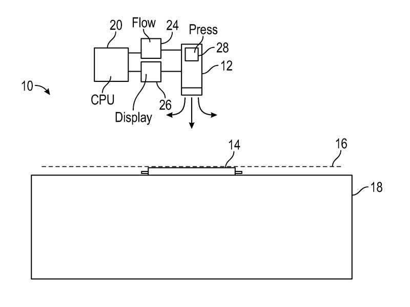
Systems and methods for teaching a location in a device programming apparatus. The X, Y, Z and angle coordinates of a pick and place nozzle are initialized, and the nozzle is moved in the X and Y coordinates to a position above the device in the location to be taught. The new X and Y coordinates of the nozzle are stored to a memory along with the initial angle coordinate. The system automatically determines the Z location of the surface of the device. The nozzle then automatically picks up the device and performs vision centering to determine the X, Y and angle offsets with respect to the initialized coordinates. The X, Y and angle offsets are used to modify the stored X, Y and angle coordinates so as to precisely determine the X and Y location of the device center as well as the device angle with respect to the system’s global reference frame.
 

Description

CROSS REFERENCES TO RELATED APPLICATIONS
This application is related to U.S. Provisional Patent Application Ser. No. 60/117,873, filed Jan. 29, 1999, entitled “IN-LINE PROGRAMMING DEVICE WITH SELF-TEACHING CAPABILITY,” and U.S. Provisional Patent Application Ser. No. 60/122,023, filed Feb. 26, 1999, entitled “PICK AND PLACE TEACHING METHOD AND APPARATUS FOR IMPLEMENTING THE SAME,” the disclosures of which are each hereby incorporated by reference in its entirety.

BACKGROUND OF THE INVENTION
The present invention generally relates to automatic configuration of semiconductor device handling equipment to accommodate multiple applications and random variations among machines and devices.

In the semiconductor industry, a considerable number of electronic devices are provided by vendors in programmable form with blank memories or unspecified connections between arrays of logic. Users can then custom configure or program the electronic devices to perform their intended function by programming them, transferring or “burning in” a sequence of operating codes into the memory, or by specifying a particular arrangement of gating logic connections.

Numerous manufacturers have developed automated machinery for handling and programming such devices. Such machinery moves blank devices from a source medium (e.g., trays, tubes, etc.) to one or more programming sites, carries out the programming operation on each device, and moves programmed devices from the programming sites to an output medium (e.g., trays, tubes, etc.).

Both to allow flexible handling of a wide variety of automated programming operations (different types of input or output media, different device package types, etc.) and to account for inevitable manufacturing variations from machine to machine, it is necessary for the equipment operator to configure (or “teach”) the automated programming machinery the precise locations from which to pick up devices and to which to place devices. This includes all input and output media locations, the locations of all programming site sockets, and any other such locations within the system.

Accurate teaching is critical to the robust operation of automated programming systems. While older, larger programmable devices are relatively insensitive to placement accuracy, modem fine pitch devices have very delicate leads and suffer damage unless placement operations are highly accurate (for instance, correct to within 0.001″).

Not all automated equipment can achieve such accurate placement. In order to do so, high-end equipment uses a technique known as vision centering. The system picks up each device with a pick and place nozzle and holds the device in the path of a series of parallel laser beams. The device is then rotated in the path of the laser beams. A bank of sensors monitors which of the beams is interrupted during the rotation of the device. This information can be processed numerically to identify the precise angle and position of the device on the pick and place nozzle. Linear encoder technology allows the system to place the nozzle at any desired location. The results of the vision centering operation allow a correction move in the lateral horizontal (i.e., X, Y) and angle coordinates to be performed so that the part can be precisely placed at the desired location.

Traditional vision centering does not assist the user in determining the correct pick and place locations. Rather, it merely enables the system to place with extreme accuracy once those locations are specified.

While the ease with which the operator can carry out the teaching operation does not directly affect the physical treatment of devices, it does affect the efficiency of system operation. Typical users of automated programming equipment are highly sensitive to system throughput (measured in correctly programmed devices per hour) and yield (defined as the percentage of devices which are correctly programmed). Furthermore, more difficult teaching techniques require more highly trained personnel that draw higher wages. As a result of all of these considerations, automated programming equipment users prefer fast, easy teaching techniques.

A variety of teaching techniques has been implemented to date. These include none, file-controlled, trial-and-error, single point downward vision teaching, and double point downward vision teaching. Each of these techniques is characterized by advantages and disadvantages when considered in terms of accuracy and ease of use.

Some equipment requires no teaching whatsoever. This equipment is simple to set up and use, but is limited to devices that are rugged and can tolerate the relatively imprecise component placement that results from inevitable manufacturing variations from machine to machine. Such equipment is normally also limited to a specific device type or a small range of types and offers little flexibility to handle new devices.

Some equipment requires no active teaching on the part of the user, but offers improved flexibility by utilizing CAD data files to determine the location of device pick and place points. Systems of this type offer more flexible handling of a variety of jobs, but are still limited to rugged components that can tolerate relatively poor placement accuracy, because this teaching technique doesn’t account for random manufacturing variations.

A wide variety of equipment is available that provides operator control over the various pick and place locations but offers no systematic technique to help the operator determine the proper settings. The operator of such equipment must pursue a trial-and-error approach until correct settings are determined. Once accurately configured, such equipment can operate very reliably, but the trial-and-error process can be very time consuming and can result in many damaged (and hence unusable) parts. Equipment of this type still normally handles only rugged devices.

Some automated device programming systems are equipped with downward vision cameras. Such a camera is mounted to the movable portion of the system and can be positioned over any point in the system workspace. The camera can “look down” on the components or component locations. The operator can observe the camera field of view on a monitor which is normally equipped with crosshairs for precise positioning. Downward vision cameras can be used in “single point” or “double point” teaching mode.

In a system that employs single point downward vision teaching, the operator positions the camera crosshairs over the estimated center of the component location to be taught and indicates via a keystroke, mouse click, or some other event that the proper position has been identified. The system then stores this position and returns to it when necessary. This approach provides better accuracy than all previously described techniques, and requires only a single camera positioning operation by the user. However, the approach requires that the operator visually estimate the proper crosshair location. This can be inaccurate unless the location being taught exhibits some kind of distinct “landmark” at the center point, which is not always the case. When such a landmark is available, systems of this type can properly handle delicate fine pitch parts, while some device damage can result in the absence of such landmarks.

Double point downward vision teaching improves upon the single point technique by allowing the user to teach two points and taking as the teach point the arithmetic average of those two points. In most systems it’s much easier to find two symmetrically located “landmarks” than to find a single landmark at the precise target location. A disadvantage of this approach, however, is that the operator must position the crosshairs twice, doubling the labor involved in the teaching process. Historically, double point downward vision teaching has provided the most reliable results and has proven most successful in handling fine pitch devices.

None of the approaches described above fully exploit the fine positioning capability of modem motion control equipment. Even the most accurate of the above methods, double point downward vision teaching, requires that the operator visually align two references (the camera crosshair and the image landmark) with one another. Human vision is not capable of performing this feat to the full accuracy of motion control hardware. The approaches that do work well require extensive operator involvement and thus admit the possibility of human error.

A much more serious limitation of all existing approaches is that none of them deal effectively with angular and vertical axis coordinates. All of the approaches described above address only the lateral horizontal components of the device location. In the above approaches, angular error is normally neglected, and the vertical coordinate must be set by the operator using visual inspection of the proximity of the pick and place nozzle to the top of the device.

SUMMARY OF THE INVENTION
Briefly, the present invention provides a new and improved technique for teaching automated programming equipment that exploits the full accuracy of the system’s pick and place capabilities while requiring minimal effort on the operator’s part. The approach requires that the operator place a device in the location to be taught. The system then picks the device up, performs vision centering measurements on the device, and uses the results of these measurements to determine the precise place coordinates for the device. This information is stored in the system in a manner that prevents the need to perform teaching for any given combination of hardware items more than once.

The teaching process begins automatically when the system, e.g., via software, recognizes that the target coordinates associated with an imminent placement have not been initialized. The system guides the operator through the steps required to determine the proper values for all four coordinates (X, Y, Z, and angle).

First, the system displays an alert box on the computer monitor identifying the location in question and instructing the user to place a device in the location. Some locations (e.g., programming site sockets) hold the device in a very well defined position. Others (e.g., device pockets in input and output media) may allow a degree of play in the device’s location. After the user has placed a device in the location, he or she must ensure that the system nozzle is roughly over the device. This subjective specification of a position by the operator does not affect the final coordinates determined by the teach process. The operator must merely be close enough to allow the system to pick the part up. When the operator is satisfied with the rough location, he or she notifies the system software to indicate permission to move to the next step.

Once the operator indicates that the vacuum nozzle is over the device, the system software takes over and begins to step the nozzle downward toward the device’s upper surface. After each step the system uses a proximity sensor to determine whether the nozzle is in contact with the device. As long as the nozzle has not made contact with the device, the downward stepping process continues. Once contact is established, this part of the teaching process is complete and the vertical position of the nozzle is stored as the Z coordinate associated with the teach process for this particular location and device.

Once the Z coordinate is established, the system is capable of picking the device from its location. In one embodiment, a vacuum nozzle is used. The device is picked up by activating the vacuum nozzle while the nozzle is in contact with the device.

The system software continues the teaching process by positioning the device in the laser align beam(s) and using the vision centering process to determine the precise X, Y, and angle offsets with respect to the nozzle. The software is also able to determine the nozzle X and Y coordinates (relative to initialized X and Y axes) using linear encoder feedback. By suitably combining the encoder readings with the laser align measurement results, the system software determines the precise X and Y location of the device center as well as the device angle with respect to the system’s global reference frame. When the measurement process is complete, the system places the device back in its original position.

According to an aspect of the invention, a method is provided for teaching a location in a device programming apparatus. The method typically comprises the steps of providing a device in the location to be taught, providing a nozzle capable of picking up the device, wherein the nozzle has an initial set of horizontal coordinates and an initial vertical coordinate, and positioning the nozzle to a first set of horizontal coordinates different from the initial set of horizontal coordinates such that the nozzle is above the device. The method also typically comprises the steps of automatically determining, with the nozzle, the vertical position of the device relative to the initial vertical coordinate, automatically determining, for each of the horizontal coordinates, offset coordinates of the center of the device relative to the nozzle, and combining the horizontal offset coordinates with the first set of horizontal coordinates so as to determine the location of the device relative to the initial set of coordinates.

According to another aspect of the invention, a method is provided for teaching a location in a device programming apparatus. The method typically comprises the steps of providing a device in the location to be taught, wherein the device has an associated identifier, determining whether teaching data associated with the identifier is stored in a memory; and if not, providing a nozzle capable of picking up the device, wherein the nozzle has an initial set of horizontal coordinates and an initial vertical coordinate, and positioning the nozzle to a first set of horizontal coordinates different from the initial set of horizontal coordinates such that the nozzle is above the device. The method also typically comprises the steps of automatically determining, with the nozzle, the vertical position of the device relative to the initial vertical coordinate, automatically determining, for each of the horizontal coordinates, offset coordinates of the center of the device relative to the nozzle, combining the horizontal offset coordinates with the first set of horizontal coordinates to produce teaching data that identifies the location of the device relative to the initial set of coordinates, and storing the teaching data to the memory in association with the device identifier.

According to yet another aspect of the invention, a device programming apparatus with self-teaching capability is provided. The apparatus typically comprises a nozzle assembly having a nozzle capable of picking up a device in a location to be taught, wherein the center of the nozzle has an initial set of horizontal coordinates and an initial vertical coordinate, and a means for positioning the nozzle to a first set of horizontal coordinates different from the initial set of horizontal coordinates such that the nozzle is above the device. The apparatus also typically comprises a means for automatically determining, with the nozzle, the vertical position of the device relative to the initial vertical coordinate, a means for automatically determining, for each of the horizontal coordinates, offset coordinates of the center of the device relative to the center of the nozzle, and a means for modifying the first set of horizontal coordinates with the horizontal offset coordinates so as to produce teaching data that identifies the location of the device relative to the initial set of coordinates.

According to a further aspect of the invention, a method is provided for teaching a location in a device programming apparatus. The method typically comprises the steps of providing a device in the location to be taught, providing a nozzle capable of picking up the device, wherein the nozzle has an initial set of coordinates defined by three orthogonal axes and an initial angle coordinate defined by a first and a second one of the three axes, and positioning the nozzle to a first set of coordinates such that the nozzle is proximal the device, wherein the first set of coordinates is different from the initial coordinates along the first and second axes. The method also typically comprises the steps of automatically determining, with the nozzle, the position of the device along the third axis relative to the initial third axis coordinate, automatically determining offset coordinates of the center of the device relative to the nozzle for each of the first and second axes coordinates and the angle coordinate, and combining the offset coordinates with the first set of coordinates and the initial angle coordinate so as to determine the location and orientation of the device relative to the initial set of coordinates and initial angle coordinate.

Reference to the remaining portions of the specification, including the drawings and claims, will realize other features and advantages of the present invention.

Further features and advantages of the present invention, as well as the structure and operation of various embodiments of the present invention, are described in detail below with respect to the accompanying drawings. In the drawings, like reference numbers indicate identical or functionally similar elements.