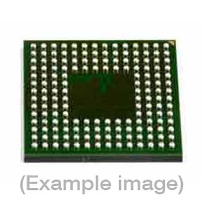
Adapters for Automated Programmers
| 6th Gen | 7th Gen | 8th Gen | 9th Gen | Flashstream |
| FASM24BGA, WASM24BGA (repl.) | FASM24BGA, WASM24BGA (repl.) | FVE4ASMC24BGJ, FVE4ASM24BGB, FVE4ASM24BGB, FVE4ASMC24BGJ | WASM24BGA | FVE4ASMC24BGJ, FVE4ASM24BGB, FVE4ASM24BGB, FVE4ASMC24BGJ |
Adapters for Manual Programmers
| 6th Gen | 7th Gen | 8th Gen | 9th Gen | Flashstream |
| FSM24BGA, FASM24BGA, WASM24BGA (repl.) | FSM24BGA, FASM24BGA, WASM24BGA (repl.) | FVE4ASMC24BGJ, FVE4ASM24BGB, FVE4ASM24BGB, FVE4ASMC24BGJ | WASM24BGA | FVE4ASMC24BGJ, FVE4ASM24BGB, FVE4ASM24BGB, FVE4ASMC24BGJ |
Adapters for Engineering Programmers
| 6th Gen | 7th Gen |
| FSM24BGA, FASM24BGA, WASM24BGA (repl.) | FSM24BGA, FASM24BGA, WASM24BGA (repl.) |
Last Updated: 05/18/2023
If the device is not yet supported by your BPM programmer (Generation), request Device Support
Note
IMPORTANT:
| Device Type: | Serial Flash with dual/quad SPI and OPI |
| Device Size: | 32M-Bit Flash Memory |
| Algorithm Programming Method: | Quad programming |
Memory Organization:
| Memory Type |
Attributes(*)
|
Included in default Range (Y/N) | DUT Physical Byte Address(hex)(if this area is selected/Activated) | BPWin Buffer Byte Address(hex) |
| Main Flash Memory | R/W/E | Yes | 0000_0000 – 003F_FFFF | 0000_0000 – 003F_FFFF |
| Security register 0 | R/W/E | Yes | 0040_0000 – 0040_00FF | 0040_0000 – 0040_0000 |
| Security register 1 | R/W/E | Yes | 0040_1000 – 0040_10FF | 0040_1000 – 0040_1FFF |
| Security register 2 | R/W/E | Yes | 0040_2000 – 0040_20FF | 0040_2000 – 0040_20FF |
| Security register 3 | R/W/E | Yes | 0040_3000 – 0040_30FF | 0040_3000 – 0040_30FF |
| Default Algorithm Range | — | — | 0000_0000 – 003F_FFFF | 0000_0000 – 003F_FFFF |
* R:Read only W: One time programmable (OTP) R/W: readable and one time programmable (OTP) R/W/E: readable and rewritable if not locked. Any configurations listed under Device-Specific’ in the menu item Device-> Settings will be written to the DUT during ‘Program’ operation regardless of memory range selection. Special Device Considerations:
| Option | Description | Default | Supported (Y/N)? |
| Status Register Protection | Protect status register. Refer to datasheet for more information. | 0 | Yes |
| Status Register | Setting a bit to 1 will protect the corresponding sector. Refer to datasheet for more information. | 0 | Yes |
| Quad Enable | Setting this bit to ENABLE will enable IO2(/WP) and IO3(/HOLD). Refer to datasheet for more information. | Disable | Yes |
| Complement Protect | It is used in conjunction with TBBP2BP1BP0 to provide for array protection. Refer to datasheet for more information. | Disable | Yes |
| Security Register Lock Bits | [LB3-LB1] are One Time Programmable(OTP). Refer to datasheet for more information. | 0 | Yes |
| WPS Bit | ‘0’ is normal WP mode. ‘1’ is individual WP mode. | 0 | Yes |
| DRV Bits | Refer to datasheet for more information. | 0 | Yes |
| HOLD or RST Function Bit | When ‘0’pin acts as /HOLD. When ‘1’pin acts as /RESET . | 0 | Yes |
| 1. | If Quad mode is set and you try to read the device it will fail read. In order to read the device Quad mode must to be enabled during programming. | |
| 2. | Please note that Security Register 0 (mapped to [40_0000-40_00FF])is reserved by Winbond for future use. It is recommended to use Security Registers 1-3 before using Register 0. | |
‘
BPM does not sell programmable devices, nor do we program devices directly. BPM makes programmers and accessories to make programming in-house fast, easy, and profitable.
Additional information
| 8-bit Bytes | 4206848 |
|---|---|
| Manufacturer | Winbond |
| Packages | BGA(24) |
| Part Number | W25Q32FVTBIG |
| Set programming | Yes |
| Vcc(program) | 3.3 |
| Package |
