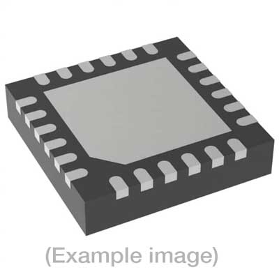
Adapters for Automated Programmers
| 8th Gen | 9th Gen |
| FVE4ASMR24QFNTA, FVE4ASMR24QFNTA | FVE4ASMR24QFNTA |
Adapters for Manual Programmers
| 8th Gen | 9th Gen |
| FVE4ASMR24QFNTA, FVE4ASMR24QFNTA | FVE4ASMR24QFNTA |
Adapters for Engineering Programmers
Last Updated: 05/18/2023
If the device is not yet supported by your BPM programmer (Generation), request Device Support
Note
IMPORTANT:
| Device Type: | Microcontroller(RL78/G11) |
| Device Size: | 16 KByte Code Flash + 2 KByte Data Flash |
| Algorithm Programming Method: | Two-wire UART |
Memory Organization:
| Memory Type |
Attributes(*)
|
Included in default Range (Y/N) | DUT Physical Byte Address(hex)(if this area is selected/Activated) | BPWin Buffer Byte Address(hex) |
| Code Flash | R/W/E | Yes | 0000_0000 – 0000_3FFF | 0000_0000 – 0000_3FFF |
| Data Flash | R/W/E | Yes | 000F_1000 – 000F_17FF | 000F_1000 – 000F_17FF |
| Default Algorithm Range | — | — | 0000_0000 – 000F_17FF | 0000_0000 – 000F_17FF |
* R:Read only W: One time programmable (OTP) R/W: readable and one time programmable (OTP) R/W/E: readable and rewritable if not locked. Any configurations listed under Device-Specific’ in the menu item Device-> Settings will be written to the DUT during ‘Program’ operation regardless of memory range selection. Special Device Considerations:
| Option | Description |
| Security Flag | Set Bit 1 to 0 will disable Boot cluster rewrite. Set Bit 2 to 0 will disable Block Erase. Set Bit 4 to 0 will disable Program.Bits 0 3 5 6 and 7 are reserved and should be set to 1s.Bit 4 can be erased through Erase.Once bit 2 is programmed to 0 the whole chip is secured and no further operations can be performed.Once Bit 1 is programmed to 0 the boot block clusters specified are secured and no further operations can be performed. |
| 1. | Boot cluster 0 is located in Clode Flash address 00000h – 00FFFh. Boot cluster 1 is located in Clode Flash address 01000h – 01FFFh. | |
| 2. | The Security Byte can be set under Device->Configure and programmed with Secure command. | |
| 3. | Configuration options will only be programmed and verified in the Secure command. | |
| 4. | This algorithm supports Firmware version V3.03 and below. | |
Addresses 000C0H to 000C3H of the flash memory of the RL78/G11 form an option byte area. After a successful Program + Verify operation subsequent stand alone operations may fail if code executes boot up internal device. Refer to user hardware manual for User option byte. ‘
BPM does not sell programmable devices, nor do we program devices directly. BPM makes programmers and accessories to make programming in-house fast, easy, and profitable.
Additional information
| 8-bit Bytes | 991232 |
|---|---|
| Manufacturer | Renesas |
| Packages | LAP(24) |
| Part Number | R5F1057AGNA |
| Set programming | Yes |
| Vcc(program) | 3.3 |
