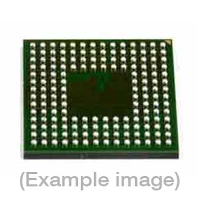
Adapters for Automated Programmers
| 9th Gen |
| FVE2ASMR256BGZ |
Adapters for Manual Programmers
| 9th Gen |
| FVE2ASMR256BGZ |
Adapters for Engineering Programmers
Last Updated: 05/18/2023
If the device is not yet supported by your BPM programmer (Generation), request Device Support
Note
IMPORTANT:
| Device Type: | LPC Microcontroller w/ARM Cortex-M3 32 bit processor |
| Device Size: | 1 MByte Flash Memory + 16 kByte of EEPROM |
| Algorithm Programming method: | SWD protocol |
Memory Organization:
| Memory Type |
Attributes(*)
|
Included in default Range (Y/N) | DUT Physical Byte Address(hex)(if this area is selected/Activated) | BPWin Buffer Byte Address(hex) |
| Flash Bank A | R/W/E | Yes | 1A00_0000 – 1A07_FFFF | 0000_0000 – 0007_FFFF |
| Flash Bank B | R/W/E | Yes | 1B00_0000 – 1B07_FFFF | 0008_0000 – 000F_FFFF |
| Default Algorithm Range | — | — | 1A00_0000 – 1A07_FFFF 1B00_0000 – 1B07_FFFF | 0000_0000 – 000F_FFFF |
* R:Read only W:One time programmable (OTP) R/W:readable and one time programmable (OTP) R/W/E:readable and rewritable if not locked. Any configurations listed under Device-Specific’ in the menu item Device-> Settings will be written to the DUT during ‘Program’ operation depending on memory range selection.Special Device Considerations:
| 1. | Auto-run code in Flash after reset available under Device Configure programs the 2’s complement of the check-sum of the remaining interrupt vectors at the Data Pattern address [0001Ch] for Flash Bank A (address 1A00001Ch in the device memory map) and the Data Pattern address [8001Ch] for Flash Bank B (address 1B00001Ch in the device memory map). | |
| 2. | Code Read Protection available under Device Configure is enabled by programming the Data Pattern address [002FCh] for Flash Bank A (address 1A0002FCh in the device memory map) and the Data Pattern address [802FCh] for Flash Bank B (address 1B0002FCh in the device memory map). It works in conjunction with the following values (Little Endian Byte Format): | |
| a. | CRP1 is enabled if value 12345678h (305419896 Decimal) is programmed. Access to chip via the JTAG pins is disabled.The following ISP commands are also disabled: Read Memory Go and Compare.The Copy RAM to Flash command cannot write to Sector 0. The Erase Sectors command can erase any sector individually except sector 0or it can erase all sectors at once. Activate flash bank is not allowed. | |
| b. | CRP2 is enabled if value 87654321h (2271560481 Decimal) is programmed. The restrictions for CRP1 apply plus the following. The following commands are disabled: Write to RAM and Copy RAM to Flash. Also the Erase command can only erase all sectors at once. | |
| c. | CRP3 is enabled if value 43218765h (1126270821 Decimal) is programmed. The restrictions for CRP2 apply plus the following. ISP entry by pulling P2_7 LOW is disabled if valid user code is present in flash sector 0. | |
| 3. | NO_ISP is enabled if value 4E697370h (1315533680 Decimal) is programmed. This disables ISP requests using the P2_7 pin. | |
| 4. | Using Code Read Protection with Auto-run code in Flash after reset for the same or both Flash banks will cause the device to become inaccessible to the programmer. | |
‘
BPM does not sell programmable devices, nor do we program devices directly. BPM makes programmers and accessories to make programming in-house fast, easy, and profitable.
Additional information
| 8-bit Bytes | 1048576 |
|---|---|
| Manufacturer | NXP Semiconductors |
| Packages | BGA(256) |
| Part Number | LPC1837FET256 |
| Vcc(program) | 3.3 |
