A “green light” doesn’t always mean the part is programmed correctly
High quality signals, Examples: Free-Running Clock (200MHz)
Have you ever had an electronic item that sometimes glitches or just stops running? Yes, you checked the batteries; it’s plugged into the wall— yet, nothing. It may not be you… You may be experiencing amnesia.
When a device loses its pattern, it’s called amnesia. Sometimes it’s called a bit-flip. It may start with just an occasional failure to boot up, but then progresses until the gadget won’t work at all. To understand how this can happen, let’s talk about how data is actually stored.
It may surprise you, but device programming is actually (more or less) analog. The basic building block of all code is a bit. Bits form bytes, and bytes form the foundation for most code. Bits are “1” or “0”, but to get that “bit” of information, we actually start much smaller—electrons.
When programming a serial flash device or MCU, every bit we store in the device is stored on a floating gate MOSFET transistor. The floating gate transistor, which is the basis of every flash device, is inherently an analog device. To get a “1” bit means it has more than a certain number of electrons stored on the gate; a “0” bit means it has fewer than that certain number. In between the “0” and the “1” lies a region of uncertainty— where the bit is going to read as a “1” sometimes and a “0” other times (not good).
Electrons are lost during the years that the device is in service due to ionizing radiation, such as gamma rays (even normal sunlight). If there are not enough electrons stored on the floating gate during programming, the device can lose its memory prematurely.
Device Life Depends on Signal Integrity
Most devices today are rated for 20 years of data retention. But, if not properly programmed, data may be lost after just a few hours, months or years, even if the device passes the initial “green light” verification.
Programmers must go to great lengths to ensure signal integrity when programming devices. It requires specialized hardware that is typically not found in less expensive programmers. The acid test— can the programmer program and test the most challenging devices, such as the AMD PALs, which are notoriously “challenging,” or antifuse FPGAs, where a single device can cost upwards of $100K each. In programming devices, it’s vital to meet every specification of the device being programmed to avoid bit flips.
Controlled impedance traces on the PCBs are critical to signal integrity. Controlled impedance is the characteristic impedance of a transmission line formed by PCB conductors. It is relevant when high-frequency signals propagate on the PCB transmission lines. Controlled impedance is important for signal integrity: it is the propagation of signals without distortion. Boards should be thoroughly tested in-house on a high-dollar oscilloscope before manufacturing. Not all of our board vendors make the grade. The problem gets down to overshoot and ringing,undershoot and rise times, and noise on these edges, set up and hold times— all these specs have to be met, or the quality of the part may prematurely degrade.
The Green Light
The green light on the socket indicates the programmer was able to verify the part. Unfortunately, it may not mean the programmer is meeting all of the device requirements. Waveform integrity has to be verified with an oscilloscope, not just the green light — it’s about meeting the specs of the device with clean waveforms for maximum quality and life expectancy.
Each part you are programming was tested and qualified on a “million-dollar” tester at the Semi House to ensure it works correctly. The device manufacturer guarantees the part will work if you meet the parts specifications. They do not test the part to ensure it will work with overshoot, ringing, ground bounce, VCC noise, ground noise, crosstalk, substrate noise, low edge rates, no bypass capacitor, setup violations, hold time violations, shorter than required programming pulses and other signal integrity problems.
When a device is programmed with inferior waveform quality, it effectively becomes a “test pilot.” How long will the data be retained? Nobody knows. It has never been tested and qualified in those conditions. Even if it passes today, that doesn’t mean it will continue to work in-circuit, with variations in voltage, temperature, timing, and the inevitable decay caused by continual bombardment from solar and terrestrial radiation sources.
One more thing to look for is “hard gold” on the PCBs. Hard gold is an extra layer of quality to ensure low resistance contacts, especially on socket cards connections between the PCB and socket. It also ensures solder connections that won’t oxidize.
The Bottom Line
Many cheap programmers are available that don’t pay attention to signal integrity
Just getting the green light on is not the same as programming the DUT correctly. It does not ensure good signal integrity.
When you don’t meet the device specs, you become a test pilot. You are operating the device in conditions it has never been tested to handle. Your results are unpredictable.
Devices can get amnesia days, months or years after programming if the programmer has poor signal integrity
Programmers with 2-layer boards, dip adapters and no active circuitry by the socket are highly suspect
To Ensure Signal Quality
Pin drivers must be are accurate enough to meet the stringent demands of eMMC programming at HS400 with 600ps rise time and fall time
Utilize premium 3GHz controlled-impedance connectors on every socket adapter
Design using controlled impedance multi-layer PCBs right up to the socket to maintain signal integrity
Test the waveform accuracy and impedance of circuit boards to ensure signal integrity
Sophisticated Oscilloscope tests should be used to confirm performance, rise time and signal integrity
Conclusion
Not all programming solutions are the same. If quality and maximum device life are important, it’s imperative to know what to look for. When evaluating a programming solution, ask about signal integrity. Go through the device specifications and demand evidence that all of the specs are being followed.
Exceptional products start with exceptional programming. Mass programming is one of the important stages in the final product build and release.
This white paper shares information to help engineers involved in the industry of eMMC device programming. It summarizes the basic specification that all eMMC devices follow including device architecture, bus protocols, modes, data read/write, and production state awareness.
The white paper also lists the criteria decision-makers should consider when evaluating the effectiveness of their Universal Programming equipment. The quality and efficiency of programming equipment affect the quality and cost of the final product as well as time to market.
Introduction
Over the past decade, the demand for high-density, nonvolatile memories with a small footprint has increased dramatically. Two of the most popular markets driving this demand are handheld devices and automotive. Demand for handheld devices continues to drive the research for high-density, low power, low-cost, high-speed, nonvolatile memories while maintaining a small footprint. NAND-type flash memory is the perfect match for such a market. The increased consumer demand for high-tech features in automobiles, such as infotainment systems, is also a big driver of demand for high-density NAND-based devices.
Flash memory is a solid-state, nonvolatile storage medium that can be electrically erased and reprogrammed. There are two types of flash memory, NAND and NOR, named after the NAND and NOR logic gates. NAND flash memory was introduced by Toshiba scientists in 1987 [1] and can be written and read in blocks. NAND flash memory was not fully utilized until recently due to its low reliability. Early NAND flash experienced bit flips, the possibility that some programmed bits read back as zero while previously programmed bits read as one, or vice versa. Bit flips introduced bad blocks over the service life of the device. With the advances in research in Error Correction Codes (ECC) [2][6][7], along with implementing new Bad Block Management (BBM) schemes [3][7], engineers were able to better detect and correct bit flips. This increased the appeal of NAND flash memory and allowed it to dominate over its more expensive rival, NOR flash memory.
The inevitable use of ECC and BBM schemes with “RAW” NAND devices leads to increased complexity when handling these devices. To avoid such difficulties, and reduce the design and time to market cost, the trend shifted to the use of “managed NAND devices”. The typical architecture of any managed NAND device includes a raw NAND memory, which is the main storage media, plus a microcontroller [5]. The microcontroller acts as the interface between the host and the raw NAND memory. It does all management tasks such as bad block management, error detection, and correction, wear leveling, and more. This helps hide the complexity of these heavy lifting tasks and frees the host (and hence the designer) to focus on application-specific tasks. Furthermore, both customers and programming houses do not need to research and provide details (and sometimes example codes) for specific ECC or BBM schemes. These are many times not easy to obtain and are IP protected. Examples of managed NAND devices include Solid State Drives (SSD), Universal Flash Storage (UFS), Secure Digital (SD) cards, and Embedded Multimedia Card (eMMC) devices.
The focus of this paper is on eMMC devices. It begins with a brief overview of the eMMC device architecture, followed by sections explaining different protocols, speed modes, and write modes supported by these devices. A section discusses the new specifications and “production state awareness” feature introduced in recent JEDEC specifications version 5.0 and later. The paper concludes with the top five tips programming centers and decision-makers should consider when purchasing high-quality programmers for programming eMMC devices.
eMMC Architecture
Embedded Multimedia Card (eMMC) devices follow a standard prepared by JEDEC and the MMC Association. This standard, widely known as JEDEC specs, defines the eMMC electrical interface and its environment and handling [4].
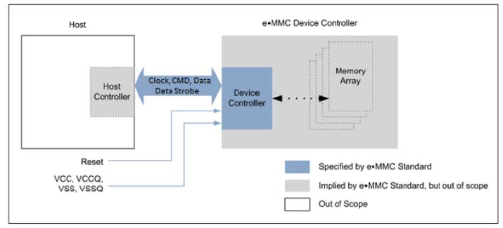
Figure 1 provides an overview of the eMMC system and the interaction between the host and device controller. The eMMC communication protocol may use up to 11-signal bus (clock, command, data strobe, and 1, 4, or 8 data buses). [4]
Figure 1. eMMC System Overview [4]
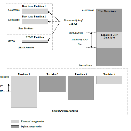
Figure 2 provides an example of partitions and user data area configuration. Upon shipping from the factory, the eMMC device consists of a user data area to store data, two boot area partitions for booting (Boot Area Partition 1 and Boot Area Partition 2), and Replay Protected Memory Block Area Partition (RPMB) to manage data in an authenticated and replay protected manner. The size of the boot area partitions and the RPMB areas are defined as multiple of 128 KB.
Figure 2. Example of partitions and user data area configuration [4]
To achieve high densities while maintaining a small footprint and lower cost per unit, NAND flash can be built using multi-level cell (MLC) flash memory. In MLC, a memory cell can store more than 1 bit. This normally creates negative effects on the chip lifetime since the risk of more bit flips could occur and decrease the number of Program/Erase cycles before the cell fails [6]. Since the boot area partitions and RPMB area are designed to hold sensitive data, these are shipped from factories in an enhanced state, also known as single-level cells (SLC). If needed, the user data area can later be enhanced. Moreover, up to four General Purpose partitions can be created, and the size and state of these areas can be adjusted by writing to a register called Extended Device-Specific Data (ECSD) register.
Bus Protocol
As described in the JEDEC specification [4], the communication between the host and the device follows a message-based bus protocol. One of the tokens described below represents each message:
Command: a command token starts operation and sends serially from the host to device on the CMD line
Response: the device sends a response token serially to the host as an answer to a previously received command on the CMD line
Data: the data lines transfer data from the device to the host or vice versa. The data bus may be set to 1(DAT0), 4(DAT0-DAT3), or 8(DAT0-DAT7)
Each token is preceded by a start bit (‘0’) and succeeded by an end bit (‘1’). Cyclic redundancy check (CRC) follows the data in each token.
Speed Mode Advancements
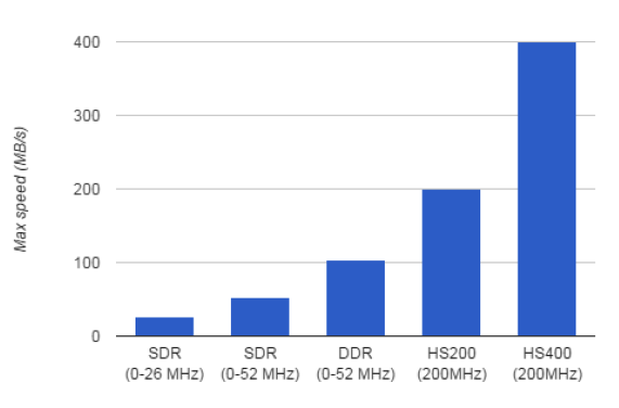
The industry has seen significant improvements in the data transfer speeds supported by eMMC devices. Figure 3 summarizes a comparison of the advancements in speed modes.
Single Data Rate (SDR)
Legacy eMMC devices support a 0-26 MHz clock speed with a maximum data transfer of 26 MB/s. They use the Single Data Rate (SDR) mode to transfer data. In this mode, a single bit can be transferred on each data line per clock cycle. Later eMMC devices support a clock speed of 0-52 MHz.
Dual Data Rate (DDR)
The 0-52 MHz eMMC devices supported the legacy SDR mode as well as a newer transfer mode introduced by JEDEC version 4.4 called Dual Data Rate (DDR). DDR mode allows the transfer of two bits on each data line per clock cycle, one per clock edge. This helps achieve a transfer rate of up to 104 MB/s. In this mode, two CRCs need to be sent after each block of data, one for bytes with an odd number and another for bytes with an even number. This totals 32 bytes, instead of 16 bytes in SDR mode, for an 8-bit data bus.
HS200
JEDEC version 4.5 introduced support for even faster clock speeds of up to 200 MHz (high-speed HS200). The maximum transfer rate for this mode is 200 MB/s.
Most recently, JEDEC version 5.0 introduced a DDR version of the HS200, known as HS400. The goal of HS400 mode is to achieve maximum data transfer to 400 MB/s (Note: that goal has been realized as of 2021).
Figure 3. Speed Mode Advancements
It is worth noting that the above speeds do not take into account the overhead of command transfers and the time taken by the device to physically write a block of data to the internal memory or prepare a block of data to be sent to the host during read operation.
Data Read/Write
The JEDEC specification defines different data read/write commands for use with eMMC.
The single block read/write – the host reads/writes a single block after issuing a “single block read/write command”
Pre-defined multiple blocks read/write – the host sets the number of blocks to be read/written followed by the multiple blocks read/write command
Open-ended multiple blocks read/write – the host continues to read/write blocks of data until it issues a stop transmission command
During the read operation, the device sends CRC after each 512 data bytes. In a similar manner, the host sends the CRC after 512 data bytes. If the CRC is correct, then the device sends back a positive CRC status “010b” to the host. Otherwise, it sends back a negative CRC status “101b” and ignores the data sent by the host. Before writing new data to any sector, the device erases the old data.
As described above, the CRC of the customer raw data file to be programmed into the device needs to be calculated. One option is to reformat the data file by embedding the CRC values after each sector. Most programmers have a tool that can perform this operation offline.
Production State Awareness
JEDEC version 5.0 introduces “Production State Awareness” to help avoid possible data corruption during soldering. Activate the Production State Awareness by setting a field in the extended CSD register before programming the part. Only a predefined part of the whole device’s available space can be supported by this feature.
5 Tips When Programming eMMC
Exceptional products start with exceptional programming. This section outlines the top five considerations manufacturers and programming centers need to look for that affect resource utilization, net throughput, and quality of programming.
1. Use HS400 Mode for High Throughput
Make sure your device programmer supports HS400 mode. To achieve high throughput, programmers need to support the highest possible speed mode currently supported by the device. JEDEC recommends HS400 mode when programming eMMC devices to achieve the highest possible programming speed. Don’t compensate for slower programming times by buying more sockets. More sockets mean higher purchasing costs, more time spent teaching, and higher maintenance costs. Faster programming times allow for fewer sockets, which creates a huge multiplier effect of time and resource savings from teaching and programming to purchasing and maintenance.
2. Ensure Clean Signal Quality for High Yield
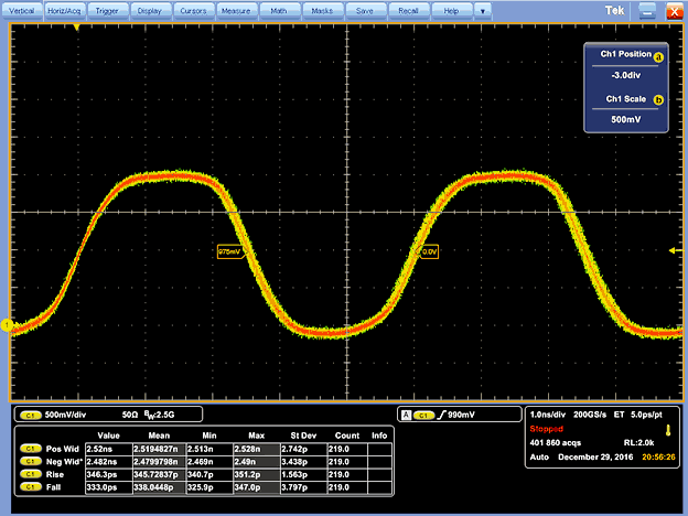
It is critical to follow programming specifications to ensure the quality of the final product. One of the signals that have crucial timing constraints in high-speed mode is the clock signal. According to JEDEC, when programming eMMC in HS400 mode the minimum pulse width must be 2.2 ns and the minimum slew rate must be 1.125 V/ns. These constraints must be maintained to achieve the highest possible speed, even if a clock period of 5 ns is used. Make sure all signals generated by your programmer follow the specification for the device. As an example, the high accuracy of the clock generated by the programmer in Figure 4 helps achieve the target transfer at a rate of 2.5 ns per byte, which puts it at the device’s limits.
Figure 4. BPM 9th Gen Clock in HS400 Mode
3. Purchase Adaptable Socket Modules for Cost Savings
Find a partner who gives you the ability to use existing socket modules for new eMMC programming instead of requiring the purchase of new socket modules. This future-thinking partner will help you smartly manage your budget. Make sure socket modules that support DDR mode also support HS400 mode, so you have high programming flexibility and keep overall costs low.
4. Invest in Automated Programmers for High Volume
To achieve high volume production in a short amount of time, consider purchasing automated programmers. High-density devices like eMMC take a longer time to program, so investing in an automated programmer allows you to increase machine utilization and maximize throughput. Look for an automated programmer equipped with a high accuracy robotic arm and cameras to ensure both accurate and careful handling of thin eMMC devices as well as other CSP devices. This will improve the speed and accuracy of handling devices during the programming process. Some automated programmers are equipped with 3D inspection systems and laser marking systems.
5. One Programmer To Rule Them All
Invest in a device programmer that supports eMMC devices as well as other types of devices. This will quickly save you time and money. A programmer that supports a high mix of devices gives you the flexibility to program different devices on a single machine. This reduces the machine idle time and setup time between different jobs since there is no need to swap programmers for different devices. In addition, there is a reduction in maintenance and training time, since you only need to train staff on operating and maintaining one machine. Finally, there are cost savings since one universal programmer will be enough to support most, if not all, of your devices. Make the decision to add additional programmers based on capacity, not device support limitations.
Summary
This paper shared knowledge about eMMC devices and programming best practices benefitting both engineers as well as decision-makers working in the industry of eMMC device programming.
The paper briefly explained the basic device specification that all eMMC devices follow: such as device architecture, protocols, speeds modes, and read/write modes.
The paper concludes with the top five characteristics to look for when purchasing an efficient eMMC programmer to maximize quality, throughput, and cost savings:
Ensure your programmer supports the highest possible speed mode (HS400 at time of writing this paper)
Ensure your programmer produces clean signal integrity
Ensure socket modules support DDR mode and HS400 mode
Invest in automated programmers to maximize volume
Ensure your programmer supports a high mix of devices
[1] S. Aritome, Kawasaki, R. Shirota, G. Hemink, T. Endoh, F. Masuoka, “Reliability issues of flash memory cells,” Proceedings of the IEEE ( Volume: 81, Issue: 5, May 1993 ).
[2] Affeldt, R., Garrigue, J., “Formalization of error-correcting codes: from hamming to modern coding theory.” In: Urban, C., Zhang, X. (eds.) ITP 2015. LNCS, vol. 9236, pp. 17–33. Springer, Heidelberg (2015). doi:10.1007/978-3-319-22102-12 4.
[3] Priyanka P. Ankolekar, Roger Isaac, and Jonathan W. Bredow, “Independent bad block management for mass storage flash memory arrays”, IEEE Transactions on Device and Materials Reliability (Volume: 10, Issue: 1, March 2010).
[4] Jedec Solid-state technology association, “Embedded Multi-Media Card (eMMC) Electrical Standard (5.1),” [https://www.jedec.org/standards-documents/docs/jesd84-b51]. http://www.jedec.org/standards-documents/results/jesd84-b51, February 2015.
[5] Sandisk, “Design Considerations for SD™ Cards and e.MMC Products”, [https://link.sandisk.com/content/dam/customer-portal/en_us/external/public/cps/collaterals/white_paper/white_paper_design_considerations_v1_0.pdf], 2015.
[6] D. Allred, G. Agarwal, “Software and hardware design challenges due to the dynamic raw NAND market”, EE Times, 2011. [7] STMicroelectronics, “Bad block management in NAND flash memories” EET Asia, 2014.
[8] Micron, “Bad Block Management in NAND Flash Memory” Technical note TN-29-59, https://www.micron.com/~/media/documents/products/technical-note/nand-flash/tn2959_bbm_in_nand_flash.pdf, 2011.
During the manufacturing of electronic systems, blank non-volatile devices must often be programmed with initial data content. This allows the target system to get up and running, and is referred to as “factory programming,” “factory pre-programming,” or “bulk programming.” Generally, this is a very straightforward process that has been in place in the industry for many years. However, with NAND flash the process is more difficult.
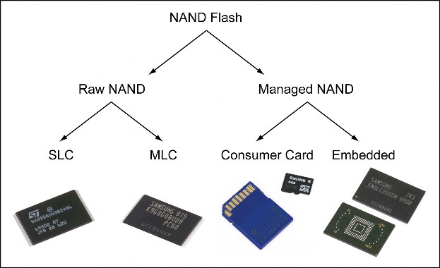
Figure 1: NAND Flash-type categories
NAND flash is a high-density, non-volatile memory that requires increased algorithm complexity during factory programming when compared to other flash memory architectures, such as NOR. This is primarily due to the existence of bad memory blocks and other reliability issues in the device shipped from the supplier. NAND flash manufacturers are able to achieve commercially viable yields by allowing a small portion of the memory to fail the test while still classifying the device as good. This tradeoff produces the very low-cost, high-density characteristics for which NAND flash is sought. By comparison, NOR flash is shipped with no such bad blocks at a much higher cost per bit and is simply not available in the densities that NAND provides. NAND flash is also superior to NOR for erase and write performance. By contrast, NOR is the fastest when it comes to reading the memory.
NAND Flash Types
To further complicate matters, there are multiple types of NAND flash as shown in Figure 1. Since programming requirements vary amongst the different types, it is important to be capable of identifying these NAND types. There are two main categories: Raw and Managed. Raw NAND is the most cost-effective since it contains just the flash memory array and a Program/Erase/Read (P/E/R) controller. However, extra processing power and complexity are needed in the target embedded system to manage the raw NAND and make it reliable. Managed NAND on the other hand, contains a more sophisticated controller that internally manages the NAND. This typically increases the cost over raw NAND for the same memory density but makes the NAND much easier to integrate.
Raw NAND is available in two types: Single-Level Cell (SLC) and Multi-Level Cell (MLC). The basic difference between the two is the number of data bits each memory cell holds. For SLC, exactly one bit of information is held in each memory cell. MLC devices store two or more bits per cell, though this is not without tradeoff. By storing more bits per cell, the storage capacity of the NAND can be doubled, quadrupled, or even more for roughly the same cost to produce the die as compared to SLC. Looking at it another way, MLC can produce the same storage capacity as SLC but using a smaller die, and therefore at a lower cost.
The most recognized managed NAND devices are consumer card types. Popular card types include CompactFlash (CF), Secure Digital (SD), and MultiMediaCard (MMC), just to name a few. These ubiquitous memory cards are sold direct to consumers for applications such as portable music players, digital cameras, handheld computers, and mobile phones. The card packaging is standards-based and is designed to withstand handling by consumers as they are inserted and removed many times from a variety of devices.
Embedded managed NAND types are electrically very similar to consumer cards, with the key difference being in the packaging. Embedded managed NAND devices are designed to be surface-mount (SMT) soldered into the target system. Such devices are a permanent part of the embedded system and are not accessible to the consumer. These devices are most often in ball grid array (BGA) style packages. Embedded managed NAND devices are becoming increasingly popular due to their ease of integration. The allure for system designers is the ability to use existing electrical interfaces designed for consumer cards. Furthermore, these devices appear the same as a consumer card to software drivers designed to interface to consumer cards. Some examples of embedded managed NAND are Samsung’s moviNAND™, Micron’s e-MMC™, SanDisk’s iNAND™, Toshiba’s eSD™, and the MultiMediaCard Association’s eMMC™.
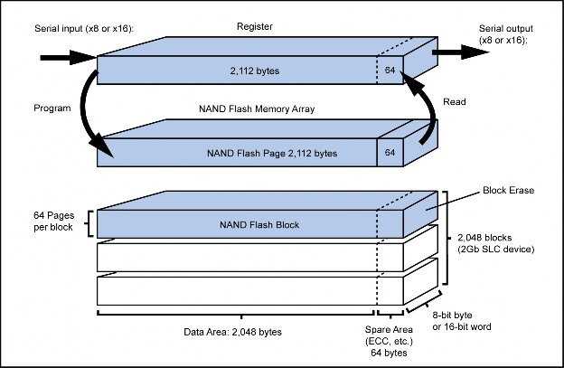
NAND Flash Memory Architecture
NAND flash is a block storage device that doesn’t utilize any address lines. Unlike NOR flash and other random access memory devices, it is not possible to read or write directly to a single data word. Reads and writes to NAND flash must be performed using multiple byte quantities called “pages.” Each page is comprised of a “main area” for data storage, and a smaller “spare area” for storing metadata to enhance the integrity of the data in the main area, among other things. This spare area is sometimes referred to as the “out-of-band” or “redundant” area. The industry standard at this time for the additional capacity of the combined spare areas is 3.125% of advertised NAND capacity. However, a few recent devices have increased this to over 5%. The trend of increasing spare area capacity will most likely continue as advertised capacities increase and the drive to reduce the cost-per-bit reduces reliability.
Block Size (pages)
Page Size (bytes)
Main Area (bytes)
Spare Area (bytes)
64
528
512
16
64
2112
2048
64
64
4224
4096
128
128
2112
2048
64
128
4224
4096
128
128
4314
4096
218
Table 1 – Typical block and page sizes.
Figure 2: NAND Flash Memory Architecture.
Read more…
continued…
Partial Page Programming
It used to be that most NAND devices would support multiple writes to a page before the page had to be erased, thus erasing all pages in the block. This is referred to as “partial page programming.” Since the entire page has to be written during program operations, 0xFF is clocked into the device for the unused locations. Later, when data needs to be written to these unused locations, the existing data and the new data are written to the page. This has the effect of programming the same data over again for the existing byte locations. Such a technique is popular in systems designed or optimized for small-page NAND (512+16), but interface to large-page NAND (2048+64).
However, with modern NAND devices, especially MLC NAND, partial page programming is not supported in the device. Re-programming the same data into a page can cause bit errors to occur either immediately or in time. For this reason, during factory programming it is important to only program pages containing data, and to program these pages exactly one time. In other words, completely blank pages should never be written to during the factory programming process. These pages should only be read and blank-checked, if desired.
Booting From NAND
NAND flash devices were originally adopted for mass storage applications, both in embedded systems and as a removable media due to large memory capacities and the lack of an address bus. Code storage and execution, especially boot-up code, were almost exclusively implemented in NOR flash. Since NOR flash has an address bus, it is a true random access device. This enables a so-called “eXecute-In-Place (XIP)” architecture, where the embedded system processor can run code directly from the NOR flash. This can be a critical requirement during the very early boot-up phase of a system. For this reason, most systems requiring bulk storage combined both NOR and NAND flash on the board. The NOR was used for critical firmware storage and execution, and the NAND for mass media and application storage similar to a mechanical hard-drive in a PC.
This paradigm is changing however, as more embedded system designs make increasing use of processors that contain integrated NAND controller hardware. These systems are capable of booting from NAND by way of a “Store and Download (SnD)” architecture. This technique involves copying the code into RAM, and then executing it from the RAM. In general, SnD on NAND is not as simple to design and factory program as XIP on NOR. However, SnD on NAND can obviate the need for the once ubiquitous NOR flash device. For cost-sensitive applications, especially consumer applications, this can be a clear winner.
NAND Flash Reliability Issues
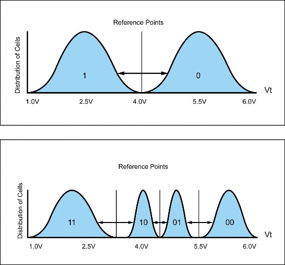
Storing information in a NAND flash cell is done by charging the cell until its threshold voltage is within a range corresponding to the data value. When reading back the cell, its threshold voltage is compared against reference points to ‘sense’ what the data value should be. For SLC, there are simply two states and a single reference point. With 2-bit MLC, there are four states and three reference points. Figure 3 illustrates this concept. It is possible to store even more bits, with more states and more reference points.
Figure 3 – SLC (top) vs. MLC (bottom) cell value distributions.
The penalty for storing more bits per cell is reduced performance and reliability. As more cell states are used, the margin of error between the cells is reduced. The programming circuitry must utilize a more complex and time-consuming algorithm to achieve a decent enough charge distribution within the error margin. Likewise, the read sense circuitry requires more time to detect the charge level within reasonable accuracy. Therefore, charging and sensing the cell voltage is not exact. Furthermore, a variety of factors will cause the threshold voltage to change over time. With SLC there is a significant margin for this error since there is only a single reference point. With MLC, this margin can become quite small. Therefore, MLC is more prone to errors than SLC.
Reliability issues come about whenever a data value is sensed differently during read-back than what the cell threshold voltage was charged to during programming for that data value. This manifests as data bits ‘flipping’ state. That is, the data output from the device does not match the original data input. But flips can occur in both SLC and MLC NAND, but MLC and its narrow margin of error are significantly more prone to bit-flip errors.
The most common cause of bit flips during factory programming is due to what’s referred to as “program disturbs.” Program disturbs occur whenever programming a region of NAND causes the threshold voltages of previously programmed cells to drift. This, however, does not always result in flipped bits. The likelihood of a program disturb resulting in a bit flip increases the more that the disturbed cell is erased. With fresh devices, which are typically used during factory programming, the cells are very resistant to the effects of program disturbs. With SLC devices and their high margin for threshold voltage error, program disturbs do not occur in fresh devices. By contrast, MLC devices will exhibit bit flips due to program disturbs even in brand new devices. With MLC, it is simply not possible to factory program the device without encountering bit errors during the verification.
It is the burden of the system interfacing to the NAND to detect and correct such bit-flip errors. This is accomplished by the use of Error Correction Codes (ECC). Before a page of data, is programmed into the NAND, an ECC algorithm is run on that data. This produces a smaller piece of metadata that can later be used to detect errors whenever the data is read back. If errors are indeed detected, the ECC is further capable of correcting the errors so long as the number of incorrect bits is less than the correction strength of the particular ECC algorithm. NAND manufacturers facilitate the storage of this extra ECC data by adding additional memory to each page in the device, referred to as the “spare area.”
In general, the number of bit errors will increase as the NAND device is worn by repeated Erase/Program cycles. So long as the bit errors remain within the system’s ECC correction capability, the data integrity is never compromised. At some point, the number of bit errors in a page may become dangerously close to exceeding what the ECC can correct. The system controlling the NAND must never allow the bit errors to exceed a correctable amount, or data loss will occur and/or the system will become defective. Therefore, entire groups of pages, called “blocks”, must be decommissioned by electrically marking them as bad. Bad blocks are never used again for data storage. Since blocks will inevitably go bad, to reduce the cost of producing NAND devices, NAND manufactures may elect to mark a certain number of blocks as bad during the die testing rather than reject the entire die. Therefore, most brand new NAND devices are shipped with known and marked bad blocks. Devices with zero bad blocks can be obtained at a very large cost, since the yield of such devices is quite low. These rare devices are sometimes referred to as “daisy samples.”
It is important to realize that NAND manufacturers do not provide any extra blocks in the devices for replacing blocks that go bad or have been factory marked bad. This is often a source of confusion with respect to the spare area. The spare area is used to store additional data needed to manage the quality of the good blocks and to make them more reliable. It is not for replacing bad blocks. When a NAND block is marked bad, the capacity of the device is permanently reduced.
Bad Block Management
Since the reliability of NAND flash will change over time as it is erased and programmed repeatedly in the target system, a scheme must be employed to manage this issue. This is referred to as bad block management (BBM). Various elements comprise a bad block management scheme, with a subset being significant during factory programming. Unfortunately, there are numerous BBM schemes used in the field, with more being devised all of the time. This adds a new dimension of complexity to programming raw NAND, because the device programmer must conduct the elements of bad block management exactly the same as the target system that the NAND device will be soldered into.
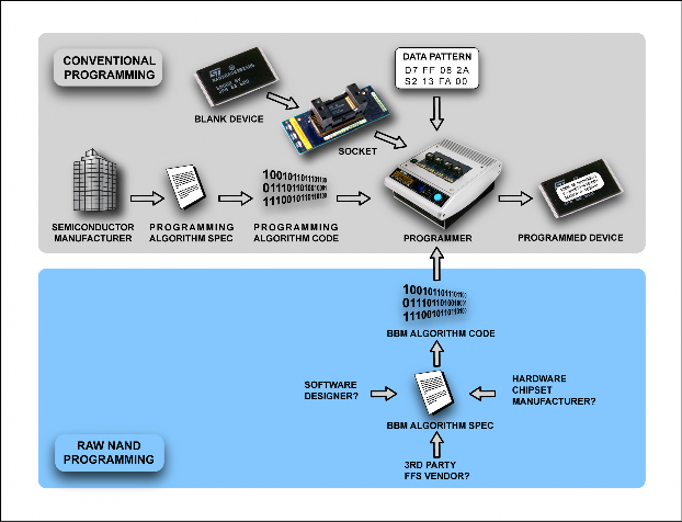
For the device programmer to support the NAND device, two algorithms are needed. The first is the conventional device programming algorithm as specified by the semiconductor manufacturer. The second is the BBM algorithm. The BBM algorithm is a user-selectable software module that interfaces with the device programming algorithm. Its implementation depends upon the target system, not just the NAND device. The challenge is in obtaining a well-defined BBM algorithm specification. Figure 4 illustrates the conventional programming support paradigm, along with the additional BBM algorithm required to program the NAND so that it will function correctly in-circuit.
Figure 4 – Conventional programming requires one algorithm for the device. Raw NAND programming requires two distinct algorithms.
When configuring a raw NAND programming job, you must select two algorithms: one for the device, and another for the BBM scheme. Unfortunately, if the BBM scheme is incorrect for the target system, there will be no sign of an issue until the devices are soldered into the circuit. There is not a safety mechanism like the device algorithm’s use of the electronic identifiers to mitigate the risk of choosing the wrong algorithm.
BBM Algorithm Specification
Unlike semiconductor devices, which generally have clear and obtainable specifications furnished by the same company that produces the device, BBM algorithm specifications can be elusive. The BBM algorithm is defined by system modules external to the NAND device, which can be hardware and/or software components. To further complicate matters, various system components can contribute a portion of the larger algorithm. These components can be from multiple suppliers. Obtaining a comprehensive BBM algorithm specification from a sole source may not be achievable. Components that may contribute to the BBM scheme include, but aren’t limited to:
commercial, open-source, or proprietary flash file system software and drivers, microcontrollers or chipsets with integrated NAND controller hardware, and hardware IP core NAND controllers.
Quite often, system designers are abstracted away from the details of all or a portion of the BBM scheme elements taking place in their design. This intellectual property might even belong to someone else. Many hardware and software vendors will not disclose the details of their BBM algorithms, or at the very least, require time-consuming non-disclosure agreements (NDA) to be executed before furnishing the specifications.
For these reasons, bad block management is often the greatest obstacle to ramping up production programming of NAND. These roadblocks must be addressed during the product design phase. If left unaddressed until the production phase, delays can occur. It can be devastating to a project schedule to discover that an incorrect BBM algorithm was used during factory programming after the devices are soldered onto the boards, and to make matters worse, nobody can come up with the BBM algorithm specification.
Six BBM Factory Programming Elements
To help with specifying BBM algorithms for production programming, six areas are important. These include:
Bad Block Replacement Strategy
Partitioning
Error Correction Codes (ECC)
Spare Area Placement
Free Good Block Formatting
Dynamic Metadata
There are other aspects of bad block management, such as wear leveling, block reconditioning, and garbage collection that are important for the target system to implement. However, only the above-listed areas are a requirement during factory programming.
Bad Block Replacement Strategy
The bad block replacement strategy defines what the algorithm must do whenever a bad block is encountered. During factory programming, these bad blocks are the result of reading the semiconductor manufacturer’s bad block indicators from the device. The strategy algorithm is responsible for locating the data originally destined for the bad block into an alternate good block. There are two fundamental bad block replacement strategies used during programming: Skip Bad Blocks and Reserve Block Area.
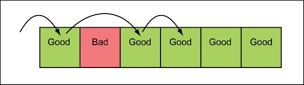
The Skip Bad Blocks replacement strategy is the most basic and straightforward replacement strategy. When a bad block is encountered, the algorithm simply skips ahead to the next good block. Figure 5 demonstrates this approach. This is the most prevalent method used during programming, as it is a very generic and well-performing strategy. It does have the side effect of causing a shift to occur between the physical and logical arrangement of data. This often requires the use of partitioning to resolve. The Skip Bad Blocks replacement strategy is not well suited for use in the target system application if the NAND will undergo extensive read/erase/write cycles since bad blocks that manifest in the field would require subsequent data blocks to shift over physically. For this reason, many flash file systems are factory programmed with Skip Bad Blocks, then resort to more complex replacement strategies at run-time. On the other hand, some applications that merely use SLC NAND in a write-seldom/read-often or ROM role simply use Skip Bad Blocks in the target system itself, since the device should not develop further bad blocks in the field during the intended use of the system.
Figure 5 – Skip Bad Blocks replacement strategy.
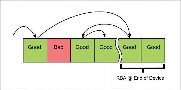
The Reserve Block Area (RBA) bad block replacement strategy utilizes a reserved “reservoir” of blocks, generally at the end of the NAND device, to be used as replacements for Bad Blocks that are encountered in the main data region, called the User Block Area. When a Bad Block is encountered during programming, the data pattern content originally destined for it is instead programmed into one of the good blocks in the RBA reservoir. This is illustrated in Figure 6. Since this strategy is not linear in nature, a table must usually be maintained that maps bad blocks to the RBA replacement block. These tables are typically proprietary to a particular bad block management scheme, and so are not generic. Some flash file systems require that the NAND device be programmed with an RBA strategy, and this can create production delays while the algorithm specification is obtained and implemented.
Figure 6 – Reserve Block Area replacement strategy.
Partitioning
Designs using NAND flash will often divide the memory into various physical regions, called partitions, much like the partitions on a PC hard-drive. One thing that partitions make possible, is the ability to guarantee that a particular piece of data will reside at a predetermined physical block, regardless of the number of bad-blocks that occur before it. This aids low-level software components such as boot-loaders and file system drivers that must easily locate the beginning of a region of data.
When utilizing Skip Bad Blocks replacement strategy, bad-blocks will cause the data to shift over into the next good block. Partitioning is required to prevent data in one region from encroaching upon adjacent regions whenever bad blocks occur, as shown in Figure 7. When utilizing an RBA style bad block replacement strategy, partitioning of the data is typically not done. Instead, the device is simply divided into User and Reserve block areas.
Defining partitions is just as essential as the data that’s going into the NAND. Partitions are a way of instructing the programmer to reject devices that are otherwise good according to specification but contain arrangements of bad blocks that will not work in the target-system. Without this additional information accurately specified, the programmer may not reject devices that would fail to function in the target-system. Partitions are expressed in terms of physical start and stop NAND blocks and the size of the image residing in the partition. Virtual device addresses can be used as an alternative to blocks. The start and stop define the physical region on the NAND device where the partition resides. The image size defines the number of good blocks required within the partition start and stop. Any NAND device not containing at least the number of good blocks defined by the image size within the partition start and stop will be rejected by the programmer.
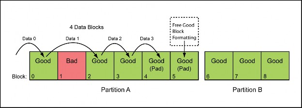
Figure 7 – Example of partition encroachment due to a bad block. The four blocks of data destined for physical NAND blocks 0-3 are interrupted by the bad physical block 1. This causes logical data block 3 to shift into partition B.
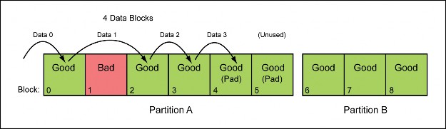
By specifying an image size that is smaller than the partition size, you are allocating ‘padding’ in the partition. The partition size is simply the number of blocks encompassed by the partition start and stop. For every padding block in the partition, there can be one bad block in the NAND device within the partition without causing the data to encroach upon the next partition. Figure 8 illustrates this concept. By creating multiple partitions with various quantities of padding, you are able to control the physical starting locations of different data regions critical to the target embedded system. Furthermore, you can tailor the padding for each partition to suit that particular partition’s usage in the end application.
Figure 8 – Preventing partition encroachment by allocating padding. Partition A contains two extra padding blocks 4 and 5. The logical data shift caused by the bad block is mitigated by these padding blocks. Data for partition B will always begin at physical block 6, as long as there are no more than 2 bad blocks in partition A.
Error Correction Codes (ECC)
ECCs are stored in the spare area of each NAND page, and allow the external system to detect data corruption in the main page area. In most cases, the ECC algorithm can correct the error. There are three ECC core algorithms predominately used for NAND Flash: Hamming, Reed-Solomon, and BCH. Furthermore, each algorithm can be parameterized in different ways to accomplish various bit correction strengths yielding a varying number of code bytes that must be written to the spare area. So long as the number of corrupt bits in a page does not exceed the number of bits the ECC can correct, the reliability of the NAND flash is upheld.
Obtaining a full ECC algorithm can be very challenging. Many system designers are unable to produce this information since the algorithm is most likely implemented in a hardware controller or commercial software library to which they do not have source code access. Often times, implementing a particular ECC algorithm may infringe upon patent rights and/or require royalties to be paid to the intellectual property (IP) holder.
Still, the factory programmer must ensure that correct ECCs are programmed into the NAND, otherwise, the target system will fail to function when the NAND is placed in-circuit. Even if the algorithm can be implemented in the programmer, generating ECCs is computationally intense requiring significant operating time. This will reduce devices-per-hour (DPH) throughput in a production programming process. During factory programming, the data pattern content is static and so the ECCs can be predetermined and embedded in the data pattern. Avoiding these computations during programming greatly increases the programming process throughput. During verification of the NAND device, the programmer is able to compare every bit read from the device to the original data pattern, which obviates the need for the ECC algorithm to detect errors.
With previous generation SLC devices, mostly 8 Gbit or less, you could rely on the factory programmed data reading back with 100% accuracy during verification. Once in-circuit, the devices could potentially exhibit bit errors after many erase/write cycles. This fundamental assumption regarding no bit flips during factory programming of fresh devices held true for many years. However, with all MLC NAND, and newer SLC NAND at around 32 Gbit and greater densities, the devices will certainly exhibit bit-flip errors during factory programming. Therefore, the device programmer must be capable of distinguishing verify errors that can be corrected in-circuit vs. errors that cannot. Only devices with bit mismatches that would fail in-circuit must be rejected, otherwise, programming yield would be reduced to zero.
For reasons described above, it is not desirable to utilize the target system’s actual ECC algorithm during factory programming, even to detect verify errors that are within the acceptable bit error rate. Instead, the device programmer can make use of a Bit Error Rate Tolerance (BERT) mechanism during verification. By simply specifying the target system’s ECC BERT per number of bytes per page to the device programmer, a high-speed verification can be achieved with specialized hardware during factory programming. This can be done without involving a particular ECC algorithm by the fact that the original data is accessible, something not true in the target system.
Spare Area Placement
The spare area of each page contains additional metadata used to manage the NAND device. Spare area placement defines this content and how it is arranged. The primary use of the spare area is for bad block markers and ECC bytes. The NAND manufacturer specifies the location of the bad block marker, and the device programmer must use these locations to recognize factory bad blocks. In practice, it is common for multiple ECCs to be used for each page. Each ECC correlates to a “sub-page,” often referred to as a sector. The spare area placement specifies the offset location of each ECC byte and the main page sector for which it corresponds.
A variety of other application-specific content can be specified in the spare area placement. Examples include erase counts, physical-logical mappings, clean markers, and garbage collection flags. However, as ECC correction requirements continue to increase, the ECCs consume more and more of the spare area. For this reason, most modern flash file systems do not add any additional metadata to the spare area beyond ECC and bad block markers.
Some system designs will deliberately violate the semiconductor manufacturer’s specified bad black mark location. It is typical of these types of systems to store non-blank data in the spare area location reserved for the bad block mark and use other criteria to indicate a bad block. It’s best to avoid such designs since these techniques don’t always transfer well to alternate NAND device part numbers. However, since many systems in the field rely on this, and if done carefully poses no problem, factory NAND programmers must support it.
Free Good Block Formatting
When using either Skip Bad Blocks or an RBA style bad block replacement strategy, there are typically unused good blocks left over in the device after programming. These are referred to as “free good blocks,” and are the result of a device containing fewer factory bad blocks than the maximum allowed by the target system design. For Skip Bad Blocks strategy, these free good blocks exist within the padding area of each partition. In an RBA style strategy, these free good blocks exist in the RBA reservoir. In either scheme, the number of free good blocks is the number of replacement blocks minus the number of actual bad blocks on the device. Usually, during factory programming, there will be some amount of free good blocks, since embedded systems are designed to withstand an increase in bad blocks that will develop in the field. Figure 9 shows an example of a free good block occurring in a skip bad blocks partition.
Figure 9 – Free Good Block Formatting specifies the content of unused blocks in a partition.
Free Good Block Formatting defines the content that the programmer must write to these blocks. Most often, this is simply blank-state that results in the programmer merely ensuring that these blocks are blank. No programming is performed within these blocks if they are to remain blank. However, some file systems do require special so-called “clean markers” or other metadata type content to be placed into the free good blocks. In this case, only the pages within the block that must contain the content are programmed. This can range from a single page up to all pages in the block. It is important for the programmer to not violate the partial page programming specification of the device. This is very important for MLC NAND devices that do not allow any partial page programming. That is, all of the bytes in a page may only be programmed a single time, with a single page programming operation. After this, no further programming on the page may be done without first erasing the entire block.
Dynamic Metadata
Some bad block management schemes require additional information specific to each device to be programmed. This dynamic metadata is usually computed by the programmer, based on characteristics unique to a particular device. The most common use of dynamic metadata is for the programming of custom, application-specific bad block remap tables and file system headers. Other uses for this data are often highly proprietary and exclusive to a particular target system design.
Example System
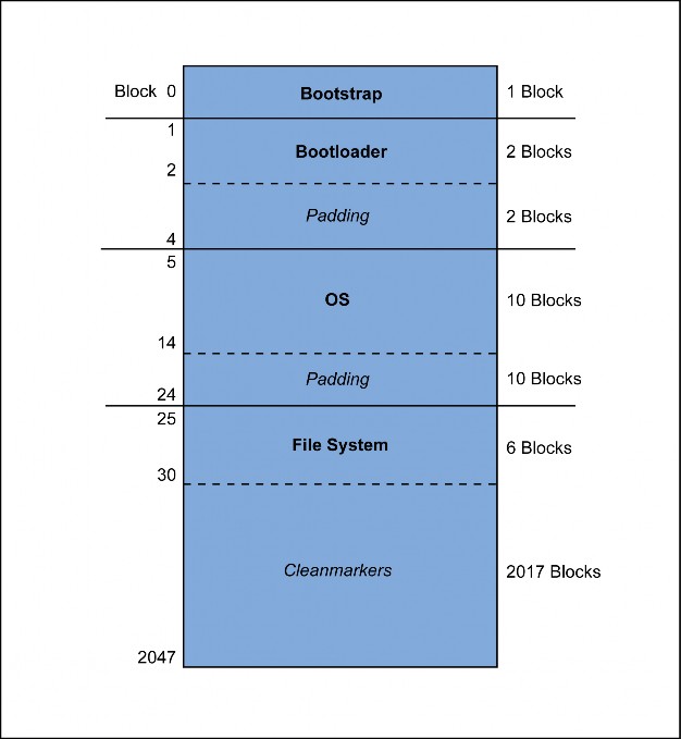
As an example, consider the following NAND Flash partition layout illustrated in Figure 10 for a Store and Download (SnD) capable system that can boot from raw NAND Flash. The system uses the Linux operating system (OS) and offers storage capabilities of media files on a JFFS2 file system on the NAND. The NAND Flash device has an organization of 2048 blocks containing 64 pages that are comprised of a 2048 byte main page with a 64-byte spare area. The NAND Flash is partitioned into 4 regions denoted by (Start-Stop:ImageSize) with the following purposes:
1. First Partition (0-0:1) – Contains the bootstrap code that the system processor’s Initial Program Load (IPL) logic will load to its internal RAM and begin executing upon reset. The partition is a single block located at block 0, without any room for Bad Blocks. The hardwired IPL logic in the processor is only capable of accessing block 0 and does not have the ability to work around bad blocks. The bootstrap’s purpose is to initialize other hardware systems (e.g. DRAM), and load the more sophisticated bootloader starting at block 1 into DRAM and transfer control to it. If this block (0) is found to be bad during pre-programming, the device must be rejected. The data in this partition is not expected to change as part of the normal use of the system. This partition occupies 1 block, starting at block 0.
2. Second Partition (1-4:2) – Contains the bootloader code that is loaded into DRAM and executed with the purpose of decompressing, loading, and executing the OS kernel. The bootloader is more significant than the bootstrap in terms of complexity and size, and so it must span 2 blocks. However, the bootstrap is capable of recognizing and skipping Bad Blocks while loading the bootloader, so this partition contains 2 reserve blocks that can be used by the device programmer to replace any Bad Blocks that occur in the first 2 blocks of the partition. The data in this partition could change and expand as updates are applied to the system, though it should be rare. This partition occupies 4 blocks, starting at block 1.
3. Third Partition (5-24:10) – Contains the compressed image of the Linux operating system kernel. This is a large region of code that is expected to be updated occasionally throughout the lifetime of the system. The bootloader will start loading the kernel into DRAM starting at block 5, skipping any bad blocks encountered. The size of the kernel image at the product launch is about 1.15MB, so it will fit into 10 blocks. An extra 10 blocks are reserved for Bad Block replacement and future expansion which are to be initialized to 0xFF. This partition occupies 20 blocks, starting at block 5.
4. Final Partition (25-2047:6) – Consumes all remaining NAND blocks, and is by far the largest partition. This is for the JFFS2 file system that contains all of the application-specific firmware, system files, and user media files. This partition is accessed by the file system driver contained in the OS kernel as a block-based storage device. The kernel will mount the file system starting at block 25. This partition will undergo heavy Read/Write cycles throughout the lifetime of the device as the user stores and manages media files and applies feature updates. The majority of this partition is unused when the product ships — the pre-programmed system only occupies 6 blocks. All remaining blocks are to provide user storage and to replace Bad Blocks in the file system. The JFFS2 driver requires that all free good blocks are programmed with “cleanmarkers” during the pre-programming process. This partition occupies 2023 blocks, starting at block 25.
Figure 10 – Example NAND Flash Memory map for an embedded system.
All partitions except the file system are Read-Only during normal usage of the end-system. For these partitions, a simple Skip Bad Blocks replacement strategy is all that is needed. The file system partition will undergo many Read-Write cycles throughout the lifetime of the end-system. Further bad block development in this partition is an expected and normal operational scenario. The file system drivers handle all of these details, including wear-leveling and idle-time garbage collection (i.e. Erase). The file system also utilizes its own Bad Block Replacement strategy that allows replacing Bad Blocks with any arbitrary block in the partition. Such a strategy is important when considering the otherwise poor performance of moving data if a Bad Block occurs between several Good Blocks. However, this does not occur during bulk pre-programming, and a simple Skip Bad Block strategy will suffice in that environment. These advanced features of the file system require complex use of Spare Area metadata in the NAND Flash device.
Universal Factory Programming BBM Scheme
To aid in a seamless design-to-manufacturing transition, the following is a highly flexible bad block management scheme to be used during factory programming that is compatible with most target systems.
Bad Block Replacement Strategy: Skip Bad Blocks
Partitions: One or more partitions defined in terms of the physical starting block, stop block, and the required good blocks on the device within each partition (image size).
ECC: All ECCs are pre-computed and contained in the data pattern file.
Spare Area Placement: All spare area bytes, including the ECCs, are contained in the data pattern.
Free Good Block Formatting: All content or blank padding for potential free good blocks is contained in the data pattern.
Dynamic Metadata: No usage of dynamic metadata.
When adhering to the above conventions during factory programming, the stock BBM algorithm can be used. This achieves the fastest throughput (DPH) without any lead-time or development fees for the BBM algorithm in the programmer. Avoiding the development of a custom BBM algorithm is very attractive since no specification is needed and there are no IP issues to overcome.
Most target systems are compatible with this scheme. Typically, the embedded system software is capable of booting from a NAND device programmed in this manner, and then it initializes a more sophisticated scheme during board bring-up. It is most common for flash file system (FFS) partitions to behave in this way. This holds true for all popular open-source FFSs and most commercial off-the-shelf (COTS) FFSs. However, there are some COTS and one-off FFSs that require an RBA style scheme during programming. These will require custom BBM algorithm development with a cost and lead-time.
The static data pattern content and layout are the main component in achieving compatibility with the Universal Factory Programming BBM Scheme. The arrangement of the data pattern should be as a flat binary file, with a 1:1 mapping to the device’s physical pages and blocks. The data content for both the main and spare area of each page must be included in sequential order just as it will be arranged physically in the device. By containing all spare area placement, including the ECCs, the data pattern can be streamed into the device very rapidly, as no computations will have to be performed on-the-fly.
The data pattern must contain all free good block formatting for all potential free good blocks. This is best understood by imagining that the NAND device doesn’t contain any bad blocks, and therefore the data pattern must have a block of data for each available block. In reality, the device programmer will discard one block of free good block formatting for each bad block encountered in a partition. Remember, even blank-state padding (0xFF) is considered free good block formatting.
Most design tools will generate a data pattern constructed according to this specification. This is the de facto image file industry standard. It is also possible to extract a data pattern meeting this standard by performing a so-called “raw” low-level read of an already programmed NAND device that contains zero bad blocks. This technique is sometimes used when a systems developer does not have the needed image file generating tools. A NAND device can be programmed using a hardware development kit using the embedded system’s software, then a raw read performed and captured into an image file. This image file can be used as the data pattern for factory programming. However, this does not capture partitioning — that information must still be specified. Some modern
design tools for NAND controllers will generate both the data pattern and a partition table file that facilitate “load and go” factory programming. There are also proprietary file formats that encapsulate the partition table and the image data. Check with your NAND controller or FFS vendor for details about their data pattern creation tools for factory programming.
Third-party and Custom BBM Schemes
Despite the industry trend towards the Universal Factory Programming BBM Scheme, there are legacy systems that are not compatible. Even some newer system designs must be factory programmed using a proprietary BBM algorithm. Manufacturing these systems is often met with delays and unexpected costs due to the non-standard BBM algorithm.
There are also COTS flash file system software libraries that do not adhere to this convention. Fortunately, these companies often produce adequate specifications for the development of the BBM algorithm for factory programming. Before choosing a commercial NAND flash file system to use in your design, ask the provider if their BBM scheme is supported by large volume production programming systems, including automated systems. Find out if they will fund the development of their BBM algorithm in the programming system of your choice. Otherwise, you may incur unexpected costs, be forced into using a single vendor’s programming solution, or worse, lack the ability to program in the volume you need at a suitably low cost.
When designing your own NAND flash controller hardware, driver software, or flash file system, be mindful of how the NAND device will be programmed during production. Don’t assume that the NAND device will be programmed in-circuit. Programming NAND in-circuit can be very costly and very slow. Furthermore, if the embedded processor must boot from NAND, then it usually needs to be programmed before it’s soldered in. For any appreciable volume, in-socket programming is usually the fastest and most economical method. Be sure that your design is capable of being programmed using the Universal Factory Programming BBM Scheme. It’s always best to switch to more complicated BBM schemes, if needed, during the first system boot after the NAND device is soldered in-circuit.
Programming Managed NAND
Factory programming managed NAND is much simpler than raw NAND, even for embedded applications. Internally, the managed NAND device contains raw SLC or MLC NAND flash. There is also a NAND controller integrated into the device, which completely manages the raw NAND access. Since managed NAND implements the BBM scheme internally, the device programmer is not burdened with this additional algorithm. For this reason, managed NAND devices are programmed in a simple and straightforward manner similar to conventional non-volatile memory devices.
The standardized managed NAND interfaces, such as SD and MMC require the use of cyclic redundancy codes (CRCs) during all transactions with the device. This stems from the concept of using memory cards, where the electrical connection is a socket accessible to the user, and thus warrants an additional layer of error detection. Though surface mount embedded devices based on these standards do not have these connection risks, the use of the CRCs is still required since it’s an inherent part of the interface. This allows for easy integration into an embedded system using existing hardware and software modules. For the highest throughput (DPH) in factory programming, it can be beneficial to pre-compute all CRCs and place them in the data pattern following each sector. This can be accomplished with an image formatter software tool. This allows the programmer to rapidly stream the data when programming and verifying. Any programming errors will be detected during the verification pass.
Serializing NAND
When factory programming any non-volatile device, it’s often necessary to program some unique data into every device. This can include examples such as simple serial numbers, network addresses, encryption keys, or even larger blocks of data constructed just-in-time. In general, the serialized data size is small compared to the entire data set being programmed. When serializing raw NAND, it may be necessary to update one or more ECCs in addition to the serialized data itself. This is required if the region being serialized is covered by an ECC. If the location being serialized is not covered by an ECC in the target system, then this additional update isn’t needed. Likewise, if serializing managed NAND devices, you may need to also update the CRC embedded in the data pattern, if the file has been pre-formatted.
Conclusion
Factory programming raw NAND flash is more complex than conventional non-volatile devices. As embedded system designers increasingly choose to use NAND flash to replace NOR, more of it will need to be factory programmed in-socket prior to assembly. Understanding how the target system requires the NAND to be programmed is critical to producing devices that will function in-circuit. Collectively known as bad block management (BBM), these six elements must be implemented in the software of the device programmer. Though de facto standards are emerging, a large number of systems have unique and esoteric requirements. For a successful ramp-up of volume production programming, obtain comprehensive BBM algorithm specifications for your project as soon as possible. Strive to achieve compatibility with the Universal Factory Programming BBM Scheme. However, if your project requires a special BBM algorithm, contact your device programmer vendor for a custom solution.
This website uses cookies to improve your experience. We'll assume you're ok with this, but you can opt-out if you wish.AcceptRejectRead More
Cookies Policy
Privacy Overview
This website uses cookies to improve your experience while you navigate through the website. Out of these cookies, the cookies that are categorized as necessary are stored on your browser as they are essential for the working of basic functionalities of the website. We also use third-party cookies that help us analyze and understand how you use this website. These cookies will be stored in your browser only with your consent. You also have the option to opt-out of these cookies. But opting out of some of these cookies may have an effect on your browsing experience.
Necessary cookies are absolutely essential for the website to function properly. This category only includes cookies that ensures basic functionalities and security features of the website. These cookies do not store any personal information.
Any cookies that may not be particularly necessary for the website to function and is used specifically to collect user personal data via analytics, ads, other embedded contents are termed as non-necessary cookies. It is mandatory to procure user consent prior to running these cookies on your website.

 Each part you are programming was tested and qualified on a “million-dollar” tester at the Semi House to ensure it works correctly. The device manufacturer guarantees the part will work if you meet the parts specifications. They do not test the part to ensure it will work with overshoot, ringing, ground bounce, VCC noise, ground noise, crosstalk, substrate noise, low edge rates, no bypass capacitor, setup violations, hold time violations, shorter than required programming pulses and other signal integrity problems.